In the fast-paced world of electronics, the demand for compact, high-performance devices has never been greater. This has given rise to High-Density Interconnect (HDI) technology, a cutting-edge innovation that is transforming how electronic devices are designed and manufactured. HDI PCB technology is specifically engineered to accommodate more components in a smaller space, making it ideal for modern applications such as smartphones, wearable devices, and IoT solutions.
Unlike traditional PCBs, which rely on standard vias and larger components, HDI technology incorporates advanced features such as microvias, stacked vias, and blind vias. These features enable higher component density, which is critical in today’s market where device size and performance are equally important.
HDI technology has become the cornerstone of modern electronic design, enabling engineers to push the boundaries of what is possible. Whether it’s creating thinner smartphones, more powerful wearables, or efficient IoT devices, HDI technology is the key to unlocking the potential of compact, high-performance electronics.
HDI technology is not just a passing trend; it is a necessity in modern technology. As electronic devices continue to shrink in size while increasing in complexity, the need for efficient and compact PCBs has grown exponentially. HDI technology empowers engineers to design devices that are not only smaller but also more powerful and reliable.
Consider the smartphone industry as a prime example. Smartphones are a perfect illustration of devices that demand high performance in a minimal footprint. HDI technology enables manufacturers to integrate more components into a smaller space, resulting in thinner, lighter, and more powerful devices. This is why HDI technology is ubiquitous in smartphones, wearables, and other compact electronics.
Beyond consumer electronics, HDI technology is also widely used in industries such as automotive, medical devices, and aerospace. In the automotive sector, HDI technology is integral to advanced driver-assistance systems (ADAS) and infotainment systems. In medical devices, it enables the creation of compact and reliable equipment. And in aerospace, HDI technology is used in avionics systems that require both high performance and reliability.
The versatility of HDI technology is one of its most compelling features. Whether you’re designing a high-end smartphone, a cutting-edge medical device, or an advanced aerospace system, HDI technology provides the performance and reliability you need. Its ability to handle high-speed signals, manage heat efficiently, and pack more components into a smaller space makes it an ideal choice for a wide range of applications.
One of the most significant advantages of HDI PCB technology is its ability to save space. In many applications, space is a critical constraint, and HDI technology allows engineers to design devices that are both smaller and more efficient. This is achieved through the use of microvias and stacked vias, which enable higher component density.
However, space-saving is not the only benefit of HDI PCB technology. It also offers improved signal integrity, which is essential in high-speed applications. By reducing the length of signal traces and minimizing the number of vias, HDI technology ensures that signals are transmitted more efficiently and with less interference.
Another key advantage of HDI technology is its improved thermal management. The compact design of HDI technology allows for better heat dissipation, which is particularly important in high-performance devices. This results in more stable and reliable operation, even under heavy workloads.
For manufacturers, HDI PCB technology also offers cost savings in the long run. While the initial investment in HDI technology may be higher, the benefits of improved performance, reduced size, and enhanced reliability often outweigh the costs. Additionally, the ability to design smaller and more efficient devices can lead to cost savings in manufacturing and assembly.
The benefits of HDI technology are not limited to performance and efficiency. It also offers significant advantages in terms of design flexibility. With HDI technology, engineers have the freedom to create more complex and innovative designs, enabling them to push the boundaries of what is possible. This is particularly important in industries such as aerospace and medical devices, where performance and reliability are paramount.

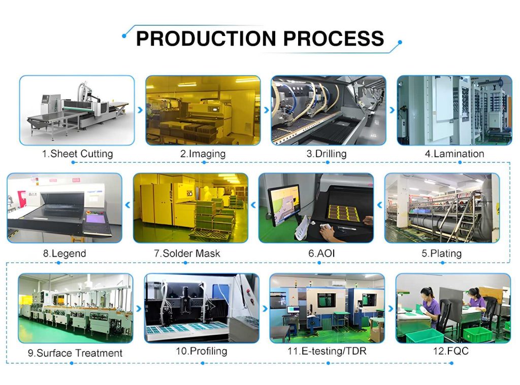
Despite its numerous benefits, HDI technology presents certain challenges for designers and manufacturers. One of the primary challenges is the complexity of the design process. HDI technology requires advanced knowledge and expertise to design effectively, as the use of microvias and stacked vias introduces additional layers of complexity.
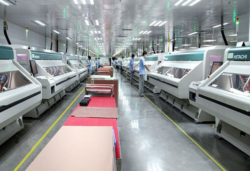
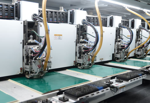
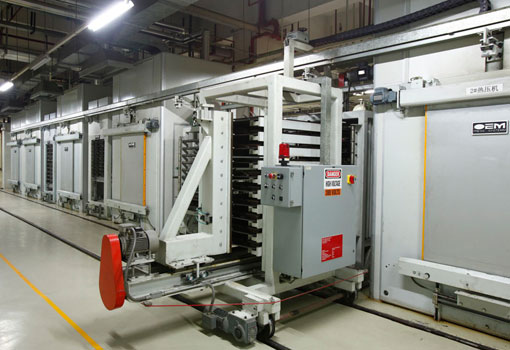
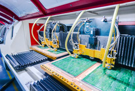
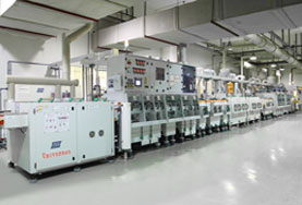
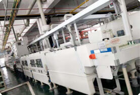
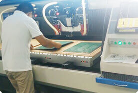
Another challenge is the manufacturing process itself. HDI technology requires precise and highly controlled manufacturing techniques to ensure that the microvias and stacked vias are created accurately. This often involves the use of advanced equipment and specialized manufacturing processes.
Additionally, the increased complexity of HDI PCB technology can lead to higher costs, both in terms of design and manufacturing. However, for many applications, the benefits of HDI technology far outweigh the challenges.
The challenges of HDI PCB technology design and manufacturing are not insurmountable, but they do require a commitment to excellence. Companies that invest in the necessary expertise and equipment can reap the benefits of HDI technology, enabling them to stay ahead of the competition and meet the demands of modern electronics.
In the consumer electronics sector, HDI technology is widely used in smartphones, tablets, and wearable devices. These devices require both high performance and a small footprint, making HDI technology an ideal choice. The compact design of HDI PCB technology allows manufacturers to create thinner and lighter devices, while the improved signal integrity ensures reliable performance.
The consumer electronics industry is highly competitive, and manufacturers are constantly looking for ways to differentiate their products. HDI technology offers a way to create devices that are not only more powerful but also more compact and user-friendly. This is particularly important in the smartphone market, where consumers demand high performance in a small package.
In the automotive industry, HDI PCB technology is used in advanced driver-assistance systems (ADAS) and infotainment systems. These systems require high performance and reliability, and HDI technology provides the necessary capabilities. Additionally, the compact design of HDI PCB technology allows for more efficient integration into vehicles.
The automotive industry is undergoing a transformation, with increasing emphasis on electrification and autonomous driving. HDI PCB technology is playing a key role in this transformation, enabling the development of advanced systems that are both powerful and reliable. From ADAS systems that enhance safety to infotainment systems that provide entertainment and information, HDI technology is at the heart of modern automotive technology.
In the medical field, HDI PCB technology is used in a wide range of devices, from diagnostic equipment to surgical tools. The compact design of HDI technology allows for the creation of smaller and more portable devices, while the improved performance ensures reliable operation.
The medical industry is focused on improving patient outcomes while reducing costs. HDI technology offers a way to create medical devices that are both more effective and more affordable. From portable diagnostic equipment that can be used in remote locations to surgical tools that are more precise and reliable, HDI technology is enabling advancements in medical technology.
In the aerospace industry, HDI PCB technology is used in avionics systems that require both high performance and reliability. The compact design of HDI technology allows for more efficient integration into aircraft, while the improved signal integrity ensures reliable operation.
The aerospace industry demands the highest standards of performance and reliability, and HDI technology is meeting those demands. From avionics systems that control navigation and communication to onboard electronics that manage power and data, HDI technology is ensuring that aerospace systems operate safely and efficiently.
At OneStopPCB, we specialize in the design and manufacturing of high-quality HDI solutions. With years of experience and a team of skilled engineers, we are committed to delivering products that meet the highest standards of quality and performance.
One of our key strengths is our ability to deliver products quickly without compromising on quality. Our streamlined processes and advanced manufacturing techniques ensure that we can meet even the tightest deadlines.
In today’s fast-paced world, speed is critical. Whether you’re developing a new product or responding to a sudden demand, you need a manufacturing partner that can deliver quickly. At OneStopPCB, we understand this, and we’ve built our processes to ensure that we can meet your needs without sacrificing quality.
We offer a wide range of HDI technology options to suit your specific needs. Whether you need standard HDI solutions or custom designs, we have the expertise and resources to deliver the perfect solution.
Every project is unique, and we recognize the importance of flexibility in meeting your specific requirements. Our team of engineers works closely with you to understand your needs and create a solution that meets your exact specifications. Whether you need a standard HDI solution or a custom design, we have the expertise to deliver.
At OneStopPCB, we prioritize customer satisfaction above all else. From the initial consultation to the final delivery, we work closely with our clients to ensure that their needs are met every step of the way.
We believe that the key to success is building strong relationships with our clients. Our customer-centric approach ensures that we understand your needs and work with you to achieve your goals. From the initial consultation to the final delivery, we are committed to providing the highest level of service and support.