
In the ever-evolving world of electronic design, engineers are constantly challenged to innovate while balancing performance, size, and cost. Traditional printed circuit boards (PCBs) have long been the backbone of electronic devices, but as technology advances, the limitations of standard PCBs have become increasingly apparent. High-Density Interconnect (HDI) PCBs have emerged as a game-changer, offering engineers a revolutionary solution to the challenges of modern design.
HDI PCBs are specifically designed to accommodate more components in a smaller space, making them ideal for applications that require high performance and a minimal footprint. These boards incorporate advanced features such as microvias, stacked vias, and blind vias, which enable higher component density and improved signal integrity. From smartphones and wearables to medical devices and aerospace systems, HDI PCBs are transforming the way engineers approach design, offering unprecedented flexibility and efficiency.

Modern electronic design is a complex endeavor, and engineers are constantly pushed to innovate while overcoming a variety of challenges. One of the primary challenges is the need for compact designs. As devices become smaller, the ability to integrate more components into a limited space becomes increasingly difficult. Traditional PCBs often struggle to meet this demand, as they rely on standard vias and larger components, which limit the overall density.
Another challenge is the need for improved signal integrity. In high-speed applications, even small amounts of signal interference can lead to significant performance issues. Traditional PCBs often require longer signal traces and more vias, which can exacerbate these problems.
Thermal management is another critical issue. As devices become more powerful, they generate more heat, which can lead to reliability issues if not managed properly. Traditional PCBs may not offer the same level of thermal efficiency as HDI PCBs, making them less suitable for high-performance applications.
Finally, there is the challenge of cost. While traditional PCBs may be cheaper to produce, they often require more space, which can lead to higher costs in other areas, such as assembly and packaging. Engineers are constantly looking for ways to reduce costs while maintaining performance, and HDI PCBs offer a solution to this dilemma.
HDI PCBs are specifically designed to address the challenges faced by engineers in modern design. One of the key advantages of HDI PCBs is their ability to accommodate more components in a smaller space. This is achieved through the use of advanced features such as microvias, stacked vias, and blind vias, which enable higher component density.
Microvias, for example, are tiny vias that are drilled directly into the PCB, allowing for more efficient routing and a smaller overall footprint. Stacked vias and blind vias further enhance this capability, enabling engineers to design devices that are both smaller and more powerful.
In addition to space-saving benefits, HDI PCBs also offer improved signal integrity. By reducing the length of signal traces and minimizing the number of vias, HDI PCBs ensure that signals are transmitted more efficiently and with less interference. This is particularly important in high-speed applications, where signal integrity is critical.
Thermal management is another area where HDI PCBs excel. The compact design of HDI PCBs allows for better heat dissipation, which is essential in high-performance devices. By managing heat more effectively, HDI PCBs ensure more stable and reliable operation, even under heavy workloads.
Finally, HDI PCBs offer cost savings in the long run. While the initial investment in HDI PCB technology may be higher, the benefits of improved performance, reduced size, and enhanced reliability often outweigh the costs. Additionally, the ability to design smaller and more efficient devices can lead to cost savings in manufacturing and assembly.
HDI PCBs are fundamentally different from traditional PCBs in several key ways. The most obvious difference is the use of advanced features such as microvias, stacked vias, and blind vias, which enable higher component density. These features are not possible with traditional PCBs, which rely on standard vias and larger components.
Another key difference is the improved signal integrity offered by HDI PCBs. By reducing the length of signal traces and minimizing the number of vias, HDI PCBs ensure that signals are transmitted more efficiently and with less interference. This is particularly important in high-speed applications, where signal integrity is critical.
Thermal management is another area where HDI PCBs excel. The compact design of HDI PCBs allows for better heat dissipation, which is essential in high-performance devices. By managing heat more effectively, HDI PCBs ensure more stable and reliable operation, even under heavy workloads.
Finally, HDI PCBs offer cost savings in the long run. While the initial investment in HDI PCB technology may be higher, the benefits of improved performance, reduced size, and enhanced reliability often outweigh the costs. Additionally, the ability to design smaller and more efficient devices can lead to cost savings in manufacturing and assembly.

Designing with HDI PCBs requires a different approach than designing with traditional PCBs. Engineers need to be familiar with the advanced features of HDI PCBs, such as microvias, stacked vias, and blind vias, and understand how to use them effectively in their designs.
One of the most important tools for HDI PCB design is specialized software. These tools allow engineers to create complex designs with microvias and stacked vias, ensuring that the final product meets all performance and reliability requirements.
Another important consideration is the need to avoid common mistakes when designing with HDI PCBs. For example, engineers need to be careful to avoid overloading the PCB with too many components, as this can lead to thermal issues. Additionally, it’s important to ensure that signal traces are as short as possible to maintain signal integrity.
HDI PCBs are used in a wide range of real-world applications, from smartphones and wearables to medical devices and aerospace systems. In each of these applications, HDI PCBs offer significant benefits, including improved performance, reduced size, and enhanced reliability.
For example, in the smartphone industry, HDI PCBs are used to create thinner, lighter, and more powerful devices. The compact design of HDI PCBs allows manufacturers to integrate more components into a smaller space, resulting in devices that are both more powerful and more user-friendly.
In the medical field, HDI PCBs are used in a wide range of devices, from diagnostic equipment to surgical tools. The compact design of HDI PCBs allows for the creation of smaller and more portable devices, while the improved performance ensures reliable operation.
In the aerospace industry, HDI PCBs are used in avionics systems that require both high performance and reliability. The compact design of HDI PCBs allows for more efficient integration into aircraft, while the improved signal integrity ensures reliable operation.
Many top engineers have successfully implemented HDI PCBs in their designs, and their experiences offer valuable lessons for others. One of the key lessons is the importance of careful planning and design. HDI PCBs require a different approach than traditional PCBs, and engineers need to be familiar with the advanced features and tools available.
Another important lesson is the need to avoid common mistakes. For example, engineers need to be careful to avoid overloading the PCB with too many components, as this can lead to thermal issues. Additionally, it’s important to ensure that signal traces are as short as possible to maintain signal integrity.
Finally, engineers need to be aware of the long-term benefits of HDI PCBs. While the initial investment may be higher, the benefits of improved performance, reduced size, and enhanced reliability often outweigh the costs.
HDI PCBs are a game-changer for engineers, offering a revolutionary solution to many of the challenges faced in modern design. From improved performance and reduced size to enhanced reliability and cost savings, HDI PCBs offer numerous benefits that make them an essential tool for engineers.
As technology continues to evolve, the demand for compact, high-performance devices will only increase. HDI PCBs are essential for meeting this demand, enabling engineers to push the boundaries of what is possible.
For engineers looking to adopt HDI PCB technology, the key is to be familiar with the advanced features and tools available, and to avoid common mistakes. With careful planning and design, HDI PCBs can help engineers create the next generation of innovative devices.
The future of electronic design is bright, and HDI PCBs will play a crucial role in driving innovation. As devices continue to shrink in size while increasing in complexity, HDI PCBs will be essential for enabling compact, high-performance designs.
From smartphones and wearables to medical devices and aerospace systems, HDI PCBs will empower engineers to create devices that are smaller, more powerful, and more reliable. The versatility of HDI PCBs makes them ideal for a wide range of applications, and their ability to handle complex designs ensures that engineers can push the boundaries of what is possible.
For engineers considering the adoption of HDI PCB technology, there are several key tips to keep in mind. First, it’s essential to invest in the right tools and software. Specialized HDI PCB design tools can help engineers create complex designs with microvias and stacked vias, ensuring that the final product meets all performance and reliability requirements.
Second, engineers should focus on careful planning and design. HDI PCBs require a different approach than traditional PCBs, and engineers need to be familiar with the advanced features and tools available. By taking the time to plan and design effectively, engineers can avoid common mistakes and create high-quality HDI PCB designs.
Finally, engineers should be aware of the long-term benefits of HDI PCBs. While the initial investment may be higher, the benefits of improved performance, reduced size, and enhanced reliability often outweigh the costs. By adopting HDI PCB technology, engineers can create devices that are smaller, more powerful, and more reliable, enabling them to stay ahead of the competition and meet the demands of modern electronics.
HDI PCBs are transforming the world of electronic design, offering engineers a revolutionary solution to the challenges of modern design. From improved performance and reduced size to enhanced reliability and cost savings, HDI PCBs offer numerous benefits that make them an essential tool for engineers.
As technology continues to evolve, the demand for compact, high-performance devices will only increase. HDI PCBs are essential for meeting this demand, enabling engineers to push the boundaries of what is possible. By adopting HDI PCB technology, engineers can create the next generation of innovative devices, driving the future of electronic design.
OneStopPCB – Your Partner in Innovation
Simplify your PCB sourcing—get in touch now for high-quality products and efficient service!
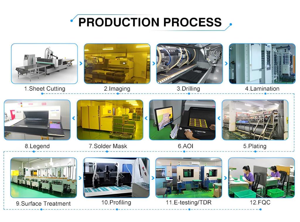
Laser drilling for microvias
Plating and deposition to ensure electrical connectivity
Lamination of multiple layers to create complex structures
Solder mask application for protection and identification
Cutting-edge tools like laser drills enable the precision required for HDI designs. Innovations in plating techniques enhance conductivity and durability.
Ensure reliability through stringent testing like electrical continuity and thermal cycling. Automated optical inspection (AOI) is also used to detect defects early.
| Specifications | PCB Capabilities |
| PCB Layers | 4 ~34 layers |
| High-Density Layers | Up to 18 layers |
| Delivery Time | 1 day to 3 weeks |
| Stackup | 1+N+1, 2+N+2, 3+N+3, 4+N+4 |
| PCB Via | Blind via, Buried via, Staggered via, Stacked via, Skip via |
| Minimum Laser Drill Diameter | 0.075mm |
| Final PCB Thickness | 0.15mm |
| Minimum Trace Width/Space | Flex/rigid-flex PCBs: 1.6mil/1.6mil Rigid PCBs: 3mil/3mil |
| Production Capability | 3000m² per day |
| Copper Thickness | 100μm to 125μm |
| Impedance Control | 90Ω ~100Ω |
| Technical Feature | 90Ω & 100Ω Differential impedance, thick cooper |
| Silkscreen | White, Black, Red,etc. |
| Soldermask | Green, Blue, Purple, White, Black, Pink,Orange |
| Surface finish | OSP, HASL, Lead Free HASL,ENIG,Immersion Tin,Immersion silver, Hard gold plating,etc. |
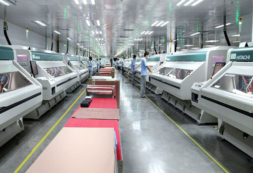
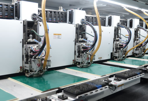
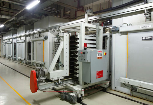
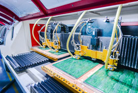
Choosing onestoppcb for your HDI PCB needs comes with numerous advantages that set us apart in the competitive electronics manufacturing industry:
Speed and Efficiency: Our streamlined manufacturing processes ensure rapid prototyping and on-time delivery, helping you maintain tight project schedules without compromise.
High Precision and Quality: Equipped with state-of-the-art facilities, we specialize in crafting high-density interconnect (HDI) PCBs with unparalleled accuracy and reliability, perfect for sophisticated and compact electronic designs.
Diverse Customization Options: Whether you need multi-layer, blind and buried vias, or microvia solutions, we offer a wide range of configurations to meet your specific requirements.
Global Trust and Expertise: With extensive experience exporting to the U.S., Europe, Vietnam, and South America, we understand and adhere to international standards, ensuring consistent quality every time.
Personalized Support: Our dedicated team of engineers and account managers work closely with you, providing expert guidance and responsive service to simplify your supply chain.
Choosing onestoppcb means partnering with a factory that values speed, diversity, and exceptional quality, ensuring your success in every project.
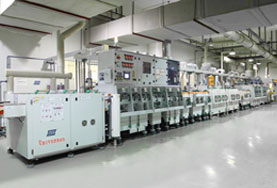

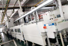
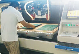
here are more pictures of our factory’s equipment display in our company profile, please click here.
● IATF 16949:2016
● ISO 9001:2015
● ISO14001:2015
● ISO13485:2016
● UL
Furthermore, all our products adhere to the IPC & ROHS Standards. It is our continuous endeavor to produce premium quality PCB products.

We understand you may have questions about our products and services. Here, we provide answers to common queries regarding our HDI PCB.
High-density interconnect, or HDI, circuit boards are printed circuit boards with a higher wiring density per unit area than traditional printed circuit boards.
HDI PCBs differ significantly from standard boards by incorporating multiple layers, micro-vias under 0.008 inches in diameter, and specialized via-in-pad processes. They often include blind, buried, and stacked vias, allowing exceptionally dense circuitry where traces and spaces both measure below 0.005 inches. This combination results in superior miniaturization and performance, making HDI PCBs ideal for mission-critical applications.
Your Trusted HDI PCB Manufacturer Since 2011
onestoppcb brings the advanced capabilities and decades of expertise required to handle all your fabrication and manufacturing needs, including high-density interconnect (HDI) PCBs. With HDI boards gaining increasing popularity across diverse sectors—such as medical, military, and aerospace—we stand ready to deliver the reliability and performance demanded by these critical industries.
PCBs built with high-density interconnect (HDI) technology generally occupy a smaller footprint, as they fit more components into a tighter space. By incorporating blind, buried, and micro vias, along with via-in-pad placements and very fine trace widths, HDI designs efficiently pack a higher component density onto a smaller board.
HDI PCBs deliver substantial advantages. They enable a more compact device footprint and can enhance overall electrical performance, supporting higher data transmission speeds. Moreover, they accommodate more input/output connections within a smaller area.
At onestoppcb, our 4-layer HDI manufacturing process closely resembles standard PCB production, with the primary distinction being the order in which holes are drilled. We start by mechanically drilling buried vias between layers 2 and 3, then move on to the through-holes from layers 1 to 4. Finally, we form blind vias between layers 1-2 and 4-3. This carefully sequenced approach ensures optimal board integrity and reliable signal performance.
At onestoppcb, we use a combination of polymer resin (dielectric)—with or without fillers—reinforcement materials, and metal foil as the primary building blocks of our circuit boards. In a typical layer construction, alternating layers of dielectric and metal foil are stacked to achieve the desired thickness and electrical performance. This process ensures both reliable functionality and structural integrity for a wide range of applications.
We’ve found that PCB dimensions and shape play a crucial role in determining cost. Larger boards require additional materials and take longer to produce, driving up expenses. Meanwhile, PCBs with unusual shapes may need specialized tooling or more complex processes, which can also contribute to higher costs
Simplify your PCB sourcing—get in touch now for high-quality products and efficient service!

ONESTOPPCB
1-4/F Property Office Building, ZhengFeng North Road, Shenzhen, China 518103
Phone: +86-0755-36309132
1-4/F Property Office Building, ZhengFeng North Road, Shenzhen, China 518103
Get in Touch with Onestoppcb – Your Premier PCB Partner
1.Fast Turnaround Time: Our streamlined manufacturing process ensures rapid prototyping and production, meeting tight deadlines effortlessly.
2Diverse Product Range: We offer an extensive variety of PCB types and designs, catering to the unique needs of engineers and procurement teams.
3Quality Assurance: With rigorous quality checks and high standards, we consistently deliver reliable and durable PCBs, minimizing risks for your projects.
Simplify your PCB sourcing—get in touch now for high-quality products and efficient service!