In today’s fast-paced world, the demand for smarter, faster devices has never been greater. From smartphones and laptops to medical equipment and automotive systems, consumers and industries alike are demanding devices that offer superior performance, speed, and reliability. High-Density Interconnect (HDI) PCBs have emerged as a key driver of this demand, enabling engineers to design devices that are not only faster but also more efficient and compact.
HDI PCBs offer a combination of advanced features, including microvias, stacked vias, and blind vias, that enable higher component density and improved performance. These features allow engineers to design devices that are faster, more powerful, and more reliable than ever before.
Smarter, faster devices are essential for a variety of reasons. First, consumers demand devices that offer superior performance and speed. Smartphones, for example, have evolved from basic communication tools to powerful computing devices that can handle complex tasks such as gaming, video editing, and artificial intelligence.
In industries such as healthcare and automotive, the need for high-performance devices is equally critical. Medical devices, for instance, must be able to process data quickly and accurately, while automotive systems require reliable performance to ensure safety and efficiency.
Finally, in the era of the Internet of Things (IoT), the demand for smarter, faster devices is only increasing. IoT devices rely on high-performance PCBs to process data and communicate with other devices, making them essential for a wide range of applications.
High-Density Interconnect (HDI) PCBs play a critical role in enabling high-performance devices. By leveraging advanced features such as microvias, stacked vias, and blind vias, HDI PCBs allow engineers to design devices that are both faster and more powerful.
HDI PCBs also offer improved signal integrity, ensuring that data is transmitted quickly and accurately. This is particularly important in high-speed applications, where even small delays can lead to significant performance issues.
Finally, HDI PCBs offer better thermal management, ensuring that devices remain stable and reliable even under heavy workloads. This is particularly important in high-performance applications, where heat dissipation is a critical factor.
One of the key benefits of HDI PCBs is their ability to improve signal integrity and processing speed. HDI PCBs use advanced routing techniques, such as microvias and stacked vias, to reduce signal path lengths and improve signal integrity. This allows for faster data transmission and processing, resulting in devices that are both faster and more reliable.
HDI PCBs also offer improved thermal management, ensuring that devices remain stable and reliable even under heavy workloads. This is particularly important in high-performance applications, where heat dissipation is a critical factor.
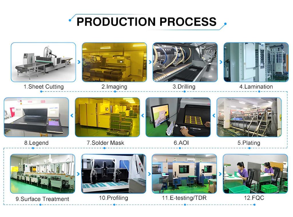
HDI PCBs are used in a wide range of devices across various industries. For example:

Designing high-performance devices is not without its challenges. Engineers must balance several factors, including speed, size, and cost. For example, while increasing the speed of a device can lead to performance improvements, it can also increase the cost and complexity of the design.
Another challenge is ensuring that the device remains compact. High-performance devices often require more components, which can make the design more complex and increase the overall size.
Finally, engineers must ensure that the device remains cost-effective. High-performance components can be expensive, and engineers must find ways to balance performance with cost.
HDI PCBs address these challenges by offering a solution that enables higher component density and improved performance. The use of microvias, stacked vias, and blind vias allows engineers to pack more components into a smaller space, resulting in devices that are both smaller and more powerful.
HDI PCBs also offer improved signal integrity, ensuring that data is transmitted quickly and accurately. This allows for faster data transmission and processing, resulting in devices that are both faster and more reliable.
Finally, HDI PCBs are increasingly being adopted in mid-range and even entry-level products, making them more accessible to a wider range of applications.
To better understand the impact of HDI PCBs on high-performance devices, let’s take a look at some real-world success stories:
A leading smartphone manufacturer approached OneStopPCB with the challenge of designing a high-performance PCB for their latest device. By leveraging our expertise in HDI PCB technology, we were able to deliver a PCB that met all of their requirements, including high performance, improved signal integrity, and reliable operation.
The result was a smartphone that was faster, more powerful, and more reliable than ever before. Our customer was thrilled with the results, and we’re proud to have played a key role in their success.
A medical device company needed a high-performance PCB for their latest diagnostic equipment. The device required high signal integrity and reliable operation, even in demanding environments.
OneStopPCB worked closely with the company to design and manufacture an HDI PCB that met all of their requirements. The result was a medical device that performed reliably, even under heavy workloads. Our customer was impressed with the quality and performance of the PCB, and we’re proud to have helped them bring their product to market.
An automotive company needed a high-performance PCB for their latest ADAS system. The device required high signal integrity and reliable operation, even under extreme conditions.
OneStopPCB worked closely with the company to design and manufacture an HDI PCB that met all of their requirements. The result was an ADAS system that performed reliably, even under extreme conditions. Our customer was impressed with the quality and performance of the PCB, and we’re proud to have helped them bring their product to market.
These case studies highlight the importance of HDI PCBs in enabling high-performance designs. By leveraging advanced features such as microvias, stacked vias, and blind vias, engineers can design devices that are both faster and more powerful.
Additionally, these case studies demonstrate the importance of partnering with a trusted PCB manufacturer. OneStopPCB’s expertise in HDI PCB technology, combined with our commitment to quality and customer satisfaction, makes us the ideal partner for your next project.
HDI PCBs are the key to smarter, faster devices, offering a solution that enables engineers to design devices that are both faster and more powerful. By enabling high-performance designs and delivering superior performance, HDI PCBs have become a cornerstone of modern electronic design.
Whether you’re designing a smartphone, a medical device, or an automotive system, HDI PCBs offer the performance benefits needed to succeed in today’s competitive market.
The impact of HDI PCBs on modern technology cannot be overstated. As technology continues to evolve, the demand for smarter, faster devices will only increase. HDI PCBs are essential for meeting this demand, enabling engineers to design the next generation of innovative devices.
If you’re ready to take your designs to the next level, contact OneStopPCB today. With our expertise in HDI PCB manufacturing and our commitment to quality, we’re here to help you achieve your goals. Visit www.onestop.com to learn more and get started on your next project.
By combining advanced technology with expert support, HDI PCBs and OneStopPCB are empowering engineers to design the future of electronics. Whether you’re looking to create a high-performance smartphone, a cutting-edge medical device, or a reliable automotive system, HDI PCBs and OneStopPCB are here to help you achieve your vision.
Don’t let the challenges of high-performance design hold you back. With HDI PCBs and OneStopPCB, you can design the next generation of electronics that are faster, more powerful, and more reliable than ever before. Visit www.onestop.com today to learn more and take the first step toward your next breakthrough innovation.
OneStopPCB is your partner in innovation, offering high-quality HDI PCBs that enable smarter, faster designs. With our commitment to speed, quality, and customer satisfaction, we’re here to help you bring your ideas to life. Contact us today to learn more about how we can support your next project.
In today’s fast-paced business environment, speed is a critical factor in staying competitive. For companies that rely on PCB manufacturing, the ability to deliver high-quality PCBs quickly can make all the difference. This is where OneStopPCB excels.
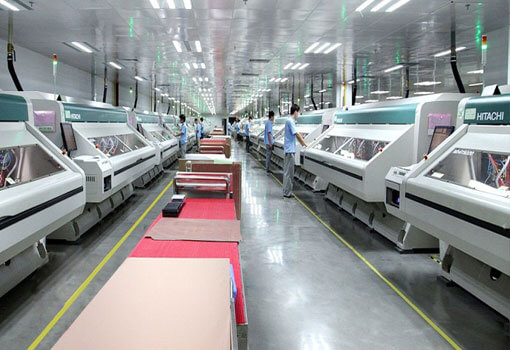
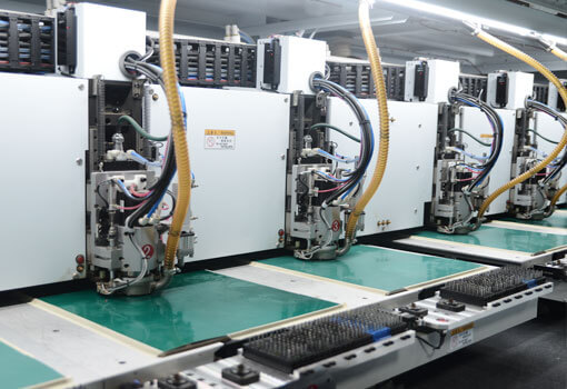
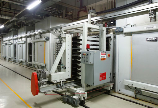
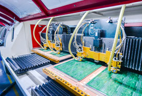
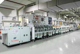
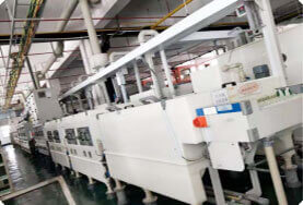
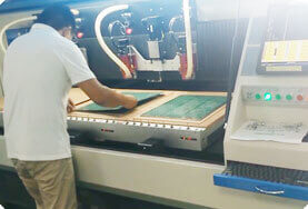
OneStopPCB is committed to delivering PCBs faster than the competition, without compromising on quality. Our state-of-the-art manufacturing facilities and streamlined processes allow us to produce high-quality PCBs in record time. Whether you’re working on a tight deadline or need to quickly prototype a new design, OneStopPCB can help you meet your goals.
Another key factor that sets OneStopPCB apart from the competition is our wide variety of PCB options. We understand that every project is unique, and that’s why we offer a diverse range of PCB types, materials, and finishes to meet the specific needs of our customers.
From standard FR-4 PCBs to advanced HDI PCBs, we have the expertise and capabilities to handle even the most complex designs. Our team of experienced engineers works closely with customers to ensure that their PCBs meet all performance and reliability requirements.
At OneStopPCB, we’re proud to have helped numerous customers achieve their goals and bring their ideas to life. Here are just a few examples of the success stories we’ve been a part of:
A leading smartphone manufacturer approached OneStopPCB with the challenge of designing a high-performance PCB for their latest device. By leveraging our expertise in HDI PCB technology, we were able to deliver a PCB that met all of their requirements, including high performance, improved signal integrity, and reliable operation.
The result was a smartphone that was faster, more powerful, and more reliable than ever before. Our customer was thrilled with the results, and we’re proud to have played a key role in their success.
A medical device company needed a high-performance PCB for their latest diagnostic equipment. The device required high signal integrity and reliable operation, even in demanding environments.
OneStopPCB worked closely with the company to design and manufacture an HDI PCB that met all of their requirements. The result was a medical device that performed reliably, even under heavy workloads. Our customer was impressed with the quality and performance of the PCB, and we’re proud to have helped them bring their product to market.
When it comes to PCB manufacturing, OneStopPCB is the clear choice for companies that demand quality, speed, and variety. Our commitment to excellence, combined with our expertise in HDI PCB technology, makes us the ideal partner for your next project.
Whether you’re designing a high-performance smartphone, a cutting-edge medical device, or a reliable automotive system, OneStopPCB has the expertise and capabilities to help you achieve your goals. Contact us today to learn more about how we can support your next project.
OneStopPCB – Your Partner in Innovation