As technology continues to evolve, the demand for high-density solutions has never been greater. Traditional PCBs (Printed Circuit Boards) have long been the backbone of electronic design, but they are increasingly unable to meet the demands of modern applications. Traditional PCBs rely on standard vias and larger components, which limit the overall density and make it difficult to create smaller, more powerful devices.
Enter High-Density Interconnect (HDI) PCBs, a revolutionary technology that is transforming the way engineers approach high-density design. HDI PCBs offer advanced features such as microvias, stacked vias, and blind vias, enabling higher component density and improved performance. This technology is not just an upgrade; it represents a paradigm shift in how electronics are designed and manufactured.
Traditional PCBs have served the electronics industry well for decades, but they are beginning to show their limitations. One of the primary challenges is their inability to meet the demands of high-density designs. Traditional PCBs rely on standard vias and larger components, which limit the overall density and make it difficult to create smaller devices.
Another limitation is the performance gap. As devices become more complex and require higher speeds, traditional PCBs often struggle to maintain signal integrity and thermal management. This is particularly problematic in high-speed applications, where even small performance issues can lead to significant problems.
Finally, traditional PCBs are often too rigid for modern applications. Many devices, such as wearables and IoT devices, require flexible designs that can adapt to different shapes and environments. Traditional PCBs are simply not flexible enough to meet these demands.
The rise of HDI PCBs has addressed many of the limitations of traditional PCBs. HDI PCBs use advanced features such as microvias, stacked vias, and blind vias to increase component density and improve performance. These features allow engineers to design devices that are both smaller and more powerful.
HDI PCBs also offer improved flexibility, making them ideal for applications that require bendable or foldable designs. This flexibility is particularly important in industries such as wearables and IoT, where devices need to adapt to different environments and use cases.
Finally, HDI PCBs offer better thermal management, ensuring that devices remain stable and reliable even under heavy workloads. This is particularly important in high-performance applications, where heat dissipation is a critical factor.

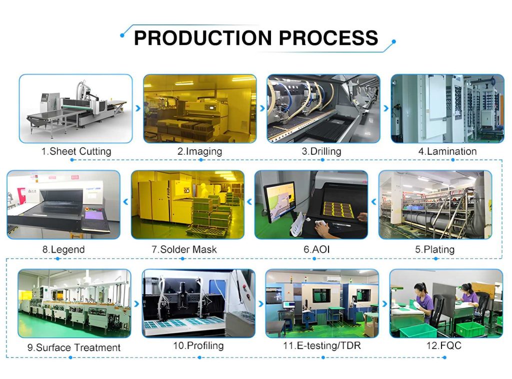
One of the key features of HDI PCBs is the use of microvias, stacked vias, and blind vias. These features allow for more efficient routing and a smaller overall footprint.
These features allow engineers to pack more components into a smaller space, resulting in devices that are both smaller and more powerful.
The advanced features of HDI PCBs enable engineers to design devices with higher component density and improved performance. By leveraging microvias, stacked vias, and blind vias, engineers can create designs that are both compact and efficient.
HDI PCBs also offer improved signal integrity, ensuring that data is transmitted quickly and accurately. This is particularly important in high-speed applications, where signal integrity is a critical factor.
Finally, HDI PCBs offer better thermal management, ensuring that devices remain stable and reliable even under heavy workloads. This is particularly important in high-performance applications, where heat dissipation is a critical factor.
HDI PCBs are being adopted across a wide range of industries, but some of the most significant applications are in smartphones, wearables, and medical devices. These industries are leading the charge in HDI PCB adoption, driven by the need for compact, high-performance devices.
In smartphones, HDI PCBs are used to create thinner, lighter, and more powerful devices. The compact design of HDI PCBs allows manufacturers to integrate more components into a smaller space, resulting in devices that are both more powerful and more user-friendly.
In wearables, HDI PCBs are used to create devices that are both compact and flexible. The flexibility of HDI PCBs allows for bendable and foldable designs, making them ideal for applications such as smartwatches and fitness trackers.
In medical devices, HDI PCBs are used to create devices that are both compact and reliable. The improved performance and reliability of HDI PCBs ensure that medical devices operate reliably, even in demanding environments.
The adoption of HDI PCBs in these industries is driven by several factors. First, these industries are characterized by rapid innovation and a constant demand for new features. HDI PCBs allow engineers to design devices that are both smaller and more powerful, enabling them to meet this demand.
Second, these industries are highly competitive, with time-to-market being a critical factor. HDI PCBs allow for faster prototyping and manufacturing, enabling companies to bring their products to market more quickly.
Finally, these industries are increasingly focused on user experience, with consumers demanding devices that are both compact and user-friendly. HDI PCBs allow for compact designs that are both powerful and easy to use, meeting the demands of today’s consumers.
As technology continues to evolve, the demand for even smaller and more powerful devices will only increase. HDI PCBs are at the forefront of this evolution, offering a solution that enables engineers to push the boundaries of what is possible.
One of the key trends in HDI PCB technology is the development of even smaller vias and more advanced routing techniques. These advancements allow for even higher component density, enabling engineers to design devices that are even smaller and more efficient.
Another trend is the integration of HDI PCBs with other advanced technologies, such as flexible PCBs and embedded components. This integration allows for even more compact designs, as well as improved performance and reliability.
Looking ahead, HDI PCBs are expected to play an even more significant role in high-density design. As technology continues to advance, the demand for compact, high-performance devices will only increase. HDI PCBs are well-positioned to meet this demand, offering a solution that enables engineers to create the next generation of innovative devices.
In the coming decade, we can expect to see even more advancements in HDI PCB technology, including the development of new materials and manufacturing techniques. These advancements will enable even higher component density and improved performance, allowing engineers to design devices that are smaller, faster, and more powerful than ever before.
HDI PCBs are essential for the future of high-density design, offering a solution that enables engineers to create devices that are smaller, faster, and more powerful than ever before. By enabling high-density designs and delivering superior performance, HDI PCBs have become a cornerstone of modern electronic design.
Whether you’re designing a smartphone, a wearable device, or a medical device, HDI PCBs offer the performance benefits needed to succeed in today’s competitive market.
The impact of HDI PCBs on modern technology cannot be overstated. As technology continues to evolve, the demand for compact, high-performance devices will only increase. HDI PCBs are essential for meeting this demand, enabling engineers to design the next generation of innovative devices.
If you’re ready to take your designs to the next level, contact OneStopPCB today. With our expertise in HDI PCB manufacturing and our commitment to quality, we’re here to help you achieve your goals. Visit www.onestop.com to learn more and get started on your next project.
By combining advanced technology with expert support, HDI PCBs and OneStopPCB are empowering engineers to design the future of electronics. Whether you’re looking to create a compact smartphone, a high-performance wearable device, or a cutting-edge medical device, HDI PCBs and OneStopPCB are here to help you achieve your vision.
Don’t let the challenges of high-density design hold you back. With HDI PCBs and OneStopPCB, you can design the next generation of electronics that are smaller, faster, and more powerful than ever before. Visit www.onestop.com today to learn more and take the first step toward your next breakthrough innovation.
OneStopPCB is your partner in innovation, offering high-quality HDI PCBs that enable compact, high-performance designs. With our commitment to speed, quality, and customer satisfaction, we’re here to help you bring your ideas to life. Contact us today to learn more about how we can support your next project.
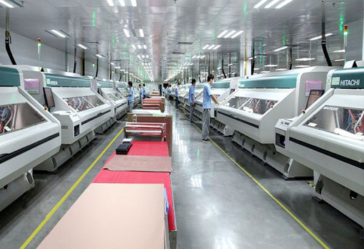
In today’s fast-paced business environment, speed is a critical factor in staying competitive. For companies that rely on PCB manufacturing, the ability to deliver high-quality PCBs quickly can make all the difference. This is where OneStopPCB excels.
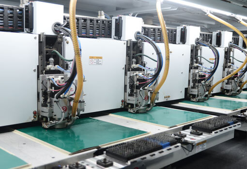
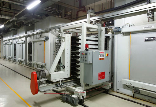
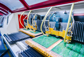
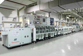
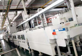
OneStopPCB is committed to delivering PCBs faster than the competition, without compromising on quality. Our state-of-the-art manufacturing facilities and streamlined processes allow us to produce high-quality PCBs in record time. Whether you’re working on a tight deadline or need to quickly prototype a new design, OneStopPCB can help you meet your goals.
Another key factor that sets OneStopPCB apart from the competition is our wide variety of PCB options. We understand that every project is unique, and that’s why we offer a diverse range of PCB types, materials, and finishes to meet the specific needs of our customers.
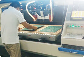
From standard FR-4 PCBs to advanced HDI PCBs, we have the expertise and capabilities to handle even the most complex designs. Our team of experienced engineers works closely with customers to ensure that their PCBs meet all performance and reliability requirements.
At OneStopPCB, we’re proud to have helped numerous customers achieve their goals and bring their ideas to life. Here are just a few examples of the success stories we’ve been a part of:
A leading smartphone manufacturer approached OneStopPCB with the challenge of designing a compact, high-performance PCB for their latest device. By leveraging our expertise in HDI PCB technology, we were able to deliver a PCB that met all of their requirements, including a compact design, high performance, and reliable operation.
The result was a smartphone that was thinner, lighter, and more powerful than ever before. Our customer was thrilled with the results, and we’re proud to have played a key role in their success.
A wearable technology company needed a high-performance PCB for their latest smartwatch. The device required a compact design and reliable operation, even in demanding environments.
OneStopPCB worked closely with the company to design and manufacture an HDI PCB that met all of their requirements. The result was a smartwatch that performed reliably, even under heavy workloads. Our customer was impressed with the quality and performance of the PCB, and we’re proud to have helped them bring their product to market.
When it comes to PCB manufacturing, OneStopPCB is the clear choice for companies that demand quality, speed, and variety. Our commitment to excellence, combined with our expertise in HDI PCB technology, makes us the ideal partner for your next project.
Whether you’re designing a compact smartphone, a high-performance wearable device, or a cutting-edge medical device, OneStopPCB has the expertise and capabilities to help you achieve your goals. Contact us today to learn more about how we can support your next project.
OneStopPCB – Your Partner in Innovation.