
In the ever-evolving world of electronics, the demand for faster, more efficient, and reliable components has never been higher. Among these components, high-frequency PCBs stand out as a cornerstone of modern technology. But what exactly makes a PCB “high-frequency,” and why is it so crucial in today’s electronics?
A high-frequency PCB is a type of printed circuit board designed to handle signals with frequencies ranging from tens of megahertz (MHz) to several gigahertz (GHz). These PCBs are engineered to maintain signal integrity, minimize signal loss, and reduce electromagnetic interference (EMI)—critical factors in high-frequency applications.
Unlike standard PCBs, which are typically used for low-frequency applications, high-frequency PCBs require specialized materials, design techniques, and manufacturing processes to ensure optimal performance.
High-frequency PCBs are the backbone of many modern technologies, enabling faster data transmission, improved signal quality, and enhanced reliability. From 5G networks and satellite communication to medical imaging and automotive radar systems, high-frequency PCBs play a vital role in supporting the demands of high-frequency, high-performance electronics.
Several industries heavily depend on high-frequency PCBs to power their innovations:
Without high-frequency PCBs, these industries would struggle to achieve the performance and reliability required for their cutting-edge technologies.
To truly understand the importance of high-frequency PCBs, it’s essential to delve into the science behind them.
At high frequencies, signals travel differently compared to low-frequency signals. High-frequency signals are more susceptible to signal loss, impedance mismatches, and electromagnetic interference (EMI).
A high-frequency PCB is designed to minimize these issues by optimizing trace lengths, widths, and spacing. Controlled impedance routing, for example, ensures that signals travel efficiently without degradation.
EMI is a major concern in high-frequency PCBs. It occurs when electromagnetic fields from external sources interfere with the signals on the PCB, leading to signal distortion or loss.
To combat EMI, high-frequency PCBs use specialized materials and design techniques. Ground planes, shielding, and proper layer stack-ups are just a few examples of how manufacturers address EMI issues.
Dielectric materials are a critical component of high-frequency PCBs. These materials, which separate the conductive layers of the PCB, affect signal integrity by influencing the speed at which signals travel and the amount of signal loss.
Materials like PTFE (Teflon) and Rogers are commonly used in high-frequency PCBs due to their low loss tangents and excellent thermal stability. These properties ensure that signals remain intact even at high frequencies.
High-frequency PCBs offer several advantages that make them indispensable in modern electronics.
One of the primary benefits of high-frequency PCBs is their ability to transmit signals quickly and with minimal loss. This is particularly important in applications like 5G networks, where data must travel across long distances without degradation.
High-frequency PCBs are designed to handle the demands of high-frequency applications, such as data centers, communication systems, and advanced radar systems. Their optimized design ensures that signals remain stable and reliable, even under high-stress conditions.
High-frequency PCBs are also engineered for better thermal management. By using materials with high thermal conductivity and incorporating advanced cooling techniques, these PCBs can dissipate heat more effectively, improving their overall reliability and longevity.
While high-frequency PCBs and standard PCBs may look similar on the surface, they are fundamentally different in terms of materials, design, and performance.
Standard PCBs are typically made from FR4, a fiberglass-reinforced epoxy material. While FR4 is cost-effective and suitable for low-frequency applications, it lacks the performance characteristics needed for high-frequency PCBs.
High-frequency PCBs, on the other hand, use advanced laminates like PTFE, Rogers, and ceramic-filled materials. These materials offer superior dielectric properties, lower loss tangents, and better thermal stability.
Standard PCBs are designed for frequencies below 1 GHz, where signal integrity is less of a concern. High-frequency PCBs, however, are built to handle frequencies up to several GHz, ensuring that signals remain intact even at high speeds.
High-frequency PCBs are more complex and costly to manufacture compared to standard PCBs. The use of advanced materials, precise design techniques, and specialized manufacturing processes all contribute to the higher cost.
Despite the higher price, the performance benefits of high-frequency PCBs often outweigh the cost, making them a worthwhile investment for many applications.
The choice of materials is critical in high-frequency PCB manufacturing. Let’s explore some of the most commonly used materials and their impact on PCB performance.
PTFE (Teflon) is a popular choice for high-frequency PCBs due to its excellent dielectric properties and low loss tangent. It is commonly used in applications like microwave circuits and satellite communication.
Rogers materials, such as Rogers 4350 and Rogers 5880, are also widely used in high-frequency PCBs. These materials offer high thermal stability, low loss tangents, and excellent dimensional stability.
The choice of material directly impacts the performance of a high-frequency PCB. Materials with low loss tangents minimize signal loss, while high thermal conductivity ensures efficient heat dissipation.
While advanced materials like PTFE and Rogers offer superior performance, they come at a higher cost. Engineers must weigh the trade-offs between cost and performance when selecting materials for their high-frequency PCBs.

Designing high-frequency PCBs is no easy task. Engineers face several challenges that require careful consideration and expertise.
One of the biggest challenges in high-frequency PCB design is controlling signal loss and ensuring proper impedance matching. Impedance mismatches can cause reflections and signal loss, leading to poor performance.
High-frequency PCBs generate more heat than standard PCBs, making thermal management a critical concern. Engineers must design PCBs with adequate cooling mechanisms to prevent overheating.
EMI and crosstalk are major issues in high-frequency PCBs. Engineers use techniques like controlled impedance routing, ground planes, and shielding to minimize these problems.
To overcome the challenges of high-frequency PCB design, engineers can follow several best practices.
Trace width and spacing play a crucial role in signal integrity. Engineers must carefully calculate these parameters to ensure proper impedance matching and minimize signal loss.
Controlled impedance routing is essential for maintaining signal integrity in high-frequency PCBs. This technique ensures that signals travel efficiently without degradation.
The layer stack-up of a high-frequency PCB is critical for signal integrity. Engineers must carefully design the stack-up to minimize crosstalk and ensure proper signal propagation.
High-frequency PCBs are integral to many modern technologies, enabling faster, more reliable performance across a wide range of industries.
5G networks rely on high-frequency PCBs to support the high data speeds and low latency required for next-generation communication.
High-frequency PCBs are used in radar systems, satellite communication, and other aerospace and defense technologies to ensure precise signal transmission.
In the medical field, high-frequency PCBs power imaging equipment like MRI machines and ultrasound devices. In automotive applications, they enable advanced driver-assistance systems (ADAS) and autonomous driving technologies.
Selecting the right manufacturer is crucial for ensuring the quality and performance of your high-frequency PCBs.
When choosing a manufacturer, consider factors like experience, expertise, and manufacturing capabilities. Look for a manufacturer with a proven track record in high-frequency PCB production.
Ensure that the manufacturer complies with industry standards like ISO 9001 and IPC-6012. These certifications indicate that the manufacturer adheres to high-quality standards.
Before placing an order, ask about the manufacturer’s experience with high-frequency PCBs, their material selection, and their quality control processes.
The future of high-frequency PCB technology is bright, with exciting advancements on the horizon.
As technology continues to evolve, the demand for faster, more efficient electronics will only increase. High-frequency PCBs will play a key role in meeting these demands.
New materials and manufacturing techniques are being developed to improve the performance and reliability of high-frequency PCBs. These advancements will enable even faster and more efficient signal transmission.
In the coming years, we can expect to see even more sophisticated high-frequency PCBs that push the boundaries of what’s possible in electronics. From 6G networks to advanced medical devices, the applications for high-frequency PCBs are endless.
High-frequency PCBs are a vital component of modern electronics, enabling faster, more reliable performance across a wide range of industries. From telecommunications and aerospace to medical devices and automotive technology, these PCBs play a critical role in supporting the demands of high-frequency, high-performance applications.
By understanding the science behind high-frequency PCBs, the challenges they face, and the best practices for designing and manufacturing them, engineers can unlock the full potential of these advanced components. As technology continues to evolve, high-frequency PCBs will remain at the forefront of innovation, driving progress and enabling new possibilities in the world of electronics.
If you’re looking for a reliable partner to help you design and manufacture high-frequency PCBs, look no further than OneStopPCB. With years of experience and a commitment to quality, we can help bring your high-frequency projects to life. Contact us today to learn more!
Simplify your PCB sourcing—get in touch now for high-quality products and efficient service!
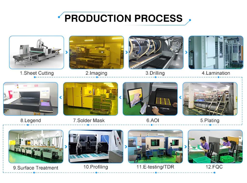
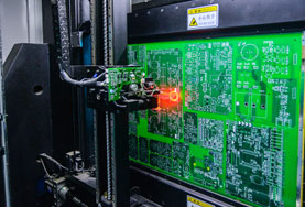
Achieving precise etching for signal traces High frequency signals demand accurate trace width control. Manufacturers use advanced etching processes and meticulous quality checks to meet tight tolerances.
Managing thermal expansion in various environments Disparate materials may expand differently under heat. Selecting compatible materials and carefully engineering the board can prevent cracks and signal losses.
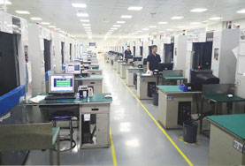
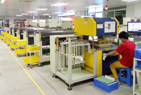
Selecting the right production partner for complex boards Partnering with a specialized manufacturer experienced in high frequency PCB production is paramount to success, ensuring efficient processes and high yields.
| Feature | Capability |
| Layer Counts | 1-36 |
| Normal Lead Time | 4-6 Working Days |
| Fast Lead Time | 1-2 Working Days |
| Materials | ISOLA, Shengyi, Rogers, Nelco, Arlon etc. |
| Copper Thickness(Finished) | 1/3OZ-20OZ |
| Overall Board Thickness | 0.2-5MM |
| Minimum Line/Track Width & Space | 3Mil/3Mil |
| Solder Mask Color | Green,black,blue.white, red,yellow. glossy and matt etc. |
| Legend/Silkscreen Color | White, yellow, black, etc |
| Back drilling | ≤16mil |
| Surface Treatment | Plating Gold, ENIG, Immersion Tin&Silver etc. |
| Qualifications | UL, ISO 14001:2015 IS9001:2015Certified |
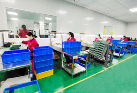
We are duly certified with the following accreditations:
● IATF 16949:2016
● ISO 9001:2015
● ISO14001:2015
● ISO13485:2016
● UL
Furthermore, all our products adhere to the IPC & ROHS Standards. It is our continuous endeavor to produce premium quality PCB products

We understand you may have questions about our products and services. Here, we provide answers to common queries regarding our HIGH FREQUENCY PCB.
High Frequency Printed Circuit Boards (HF PCBs) rely on specially engineered substrates to reliably handle signals beyond 500MHz with minimal attenuation. Thanks to this robust performance, they’re a critical component in telecom and RF microwave systems, as well as in demanding military and aerospace applications that require precision and signal integrity.
High-frequency PCBs mainly address transmission efficiency and reduced signal loss, whereas high-speed PCBs emphasize maintaining signal integrity, accurate timing, and noise mitigation. Thus, choosing the right PCB type for your specific application is vital for robust performance and reliability.
A standard guideline recommends that the ground plane extend roughly twenty times the board’s thickness (H) beyond the region of the signal traces or power planes. Essentially, this means setting the traces and power planes back by about 20H from the ground plane edges.
High-frequency electricity remains dangerous and can potentially cause severe burns. Fundamentally, it’s the voltage that drives current and causes harm, a principle that holds true regardless of frequency.
In high-frequency treatments, additional oxygen molecules are generated, yielding an antibacterial effect and a gentle warming of the tissues. This process supports blood vessels in eliminating toxins, while skin cells gain extra nutrients and increased hydration.
Signals typically operating between 50 MHz and 3 GHz are prone to issues with signal integrity, power integrity, and EMI. Therefore, when frequencies exceed 50 MHz, strict adherence to high-speed PCB design rules is crucial. Boards handling these higher frequencies are generally classified as high-speed PCBs.
Maintaining impedance control for reliability Precise impedance control is critical to prevent signal distortions. Designers must consider trace width, spacing, and layer arrangement to ensure optimal signal integrity.
Reducing interference and crosstalk issues Proper grounding and shielding techniques help to minimize electromagnetic interference, improving signal clarity and device longevity.
Effective layer stack-up strategies for optimal function Layer stack-ups can significantly influence performance. A well-planned configuration reduces interference, simplifies routing, and improves mechanical stability.
Minimizing high-frequency interference requires strategic layout, optimized layer stack-up, and precise grounding. Use continuous ground planes, keep critical traces short, and ensure each signal references a low-impedance return path. Decoupling capacitors near power pins help filter noise, while thoughtful spacing of analog and digital circuits avoids crosstalk. Proper impedance control and shielding techniques also play key roles.
Send us a message if you have any questions or request a quote. Our experts will give you a reply within 24 hours and help you select the right valve you want.

ONESTOPPCB
1-4/F Property Office Building, ZhengFeng North Road, Shenzhen, China 518103
Phone: +86-0755-36309132
1-4/F Property Office Building, ZhengFeng North Road, Shenzhen, China 518103
Get in Touch with Onestoppcb – Your Premier PCB Partner
1.Fast Turnaround Time: Our streamlined manufacturing process ensures rapid prototyping and production, meeting tight deadlines effortlessly.
2Diverse Product Range: We offer an extensive variety of PCB types and designs, catering to the unique needs of engineers and procurement teams.
3Quality Assurance: With rigorous quality checks and high standards, we consistently deliver reliable and durable PCBs, minimizing risks for your projects.
Simplify your PCB sourcing—get in touch now for high-quality products and efficient service!