In the ever-evolving landscape of modern electronics, the demand for high-frequency PCBs has surged like a relentless wave, propelled by the relentless march of technological innovation. These specialized printed circuit boards, or PCBs, are the unsung heroes behind the scenes, enabling the lightning-fast data transmission and complex signal processing that define our digital age. From the intricate dance of 5G networks to the high-stakes precision of aerospace systems, high-frequency PCBs are the backbone of a myriad of applications that shape our world.
The necessity of high-frequency PCBs is undeniable, especially in a world where the speed of data transmission is the difference between lagging behind and staying ahead. These PCBs are designed to handle the high-speed, high-frequency signals that are the lifeblood of modern communication systems. Unlike their low-frequency counterparts, high-frequency PCBs must navigate a labyrinth of challenges, from maintaining signal integrity to battling electromagnetic interference (EMI). The stakes are high, as even the slightest deviation can lead to catastrophic failures in critical applications.
The applications of high-frequency PCBs are as diverse as they are crucial. In the realm of 5G, these PCBs are the architects of the next-generation networks, enabling the ultra-fast data speeds and low latency that promise to revolutionize communication. In aerospace, high-frequency PCBs are the silent guardians of navigation systems, radar arrays, and satellite communications, ensuring that our skies remain safe and our satellites stay connected. Meanwhile, in the automotive sector, these PCBs are the driving force behind advanced driver-assistance systems (ADAS) and LiDAR technology, paving the way for autonomous vehicles and safer roads.
As technology marches forward, the demand for high-performance PCBs continues to rise. The need for faster, more reliable, and more efficient electronic systems is relentless, pushing the boundaries of what is possible. High-frequency PCBs are at the forefront of this revolution, serving as the foundation for the advanced technologies that define our modern world. From the microscopic precision of medical imaging devices to the expansive reach of global communication networks, the role of high-frequency PCBs is nothing short of transformative.
The science behind high-frequency signal transmission is a delicate dance of physics and engineering. Unlike standard PCBs, which are designed to handle low-frequency signals, high-frequency PCBs must contend with the unique challenges posed by high-speed data transmission. The key lies in the materials and design techniques used to create these PCBs, which must be carefully calibrated to ensure optimal performance. Advanced materials, such as PTFE and Rogers, play a crucial role in this process, offering the dielectric properties and thermal stability necessary for high-frequency applications.
High-frequency signal transmission is governed by principles that are both intricate and precise. The speed at which signals travel, the impedance they encounter, and the integrity they maintain are all factors that must be meticulously managed. High-frequency PCBs are designed to handle these signals with minimal loss and maximum efficiency, a task that requires a deep understanding of the underlying physics.
The differences between high-frequency and standard PCBs are profound. While standard PCBs are designed to handle low-frequency signals, high-frequency PCBs must contend with the added complexities of high-speed data transmission. This includes managing signal integrity, reducing electromagnetic interference, and ensuring proper impedance matching. The materials used in high-frequency PCBs are also more advanced, offering superior dielectric properties and thermal stability.
The materials used in high-frequency PCB design are a critical component of their success. Advanced materials, such as PTFE and Rogers, offer the dielectric properties and thermal stability necessary for high-frequency applications. These materials are carefully selected to ensure optimal performance, balancing the need for high-speed signal transmission with the challenges of thermal management and electromagnetic interference.
Designing high-frequency PCBs is a complex endeavor, fraught with challenges that demand meticulous attention to detail. Signal integrity is perhaps the most critical of these challenges, as even minor disruptions can lead to significant signal loss and impedance mismatches. Electromagnetic interference (EMI) is another constant battle, with sources ranging from nearby electronic devices to the very environment in which the PCB operates. Thermal management is equally crucial, as the high-frequency operation of these PCBs generates significant heat that must be effectively dissipated. Material selection is a balancing act, with designers forced to weigh the cost of advanced materials against the performance benefits they offer. Finally, manufacturing complexity adds another layer of difficulty, as the precision required for high-frequency PCBs is unforgiving of even the smallest errors.

Signal integrity is the cornerstone of high-frequency PCB design. High-frequency signals are notoriously sensitive to disruptions, and even minor issues can lead to significant signal loss and impedance mismatches. Designers must employ a variety of techniques to maintain signal integrity, including precise trace width and spacing, controlled impedance routing, and the use of advanced materials.
Electromagnetic interference (EMI) is a persistent challenge in high-frequency PCB design. Sources of EMI can range from nearby electronic devices to the environment in which the PCB operates. Designers must employ a variety of techniques to mitigate EMI, including the use of shielding and ground planes, as well as careful material selection.
Thermal management is a critical concern in high-frequency PCB design. The high-frequency operation of these PCBs generates significant heat, which must be effectively dissipated to prevent overheating and ensure long-term reliability. Designers must employ a variety of techniques to manage heat, including the use of advanced materials and careful layout design.
Material selection is a delicate balance in high-frequency PCB design. Advanced materials, such as PTFE and Rogers, offer superior performance but come with a higher cost. Designers must weigh the performance benefits of these materials against their cost, selecting the best option for their specific application.
Manufacturing complexity is a significant challenge in high-frequency PCB design. The precision required for these PCBs is unforgiving of even the smallest errors, and any deviation can lead to significant performance issues. Designers must work closely with manufacturers to ensure that their designs are accurately translated into high-quality PCBs.
To navigate the challenges of high-frequency PCB design, a set of best practices has emerged, offering a roadmap for success. Optimizing trace width and spacing is a foundational step, with calculations based on impedance and signal integrity guiding the design process. Layer stack-ups are another critical component, with strategies tailored to the specific requirements of high-frequency PCBs. Shielding and ground planes are essential for reducing EMI, while the selection of dielectric materials can significantly impact the overall performance of the PCB. Proper impedance matching is the linchpin of high-frequency design, ensuring that signals travel smoothly and efficiently across the board.
Optimizing trace width and spacing is a critical step in high-frequency PCB design. Designers must calculate the optimal dimensions for traces based on impedance and signal integrity, ensuring that signals travel smoothly and efficiently across the board. This requires a deep understanding of the underlying physics and careful attention to detail.
Layer stack-ups play a crucial role in high-frequency PCB design. The arrangement of layers can significantly impact signal integrity and overall performance, and designers must employ strategies tailored to the specific requirements of high-frequency PCBs. Common layer stack-up strategies include the use of multiple ground planes and carefully controlled dielectric layers.

Shielding and ground planes are essential for reducing electromagnetic interference (EMI) in high-frequency PCB design. Shielding helps to contain electromagnetic fields, while ground planes provide a low-impedance path for returning currents. Together, these elements help to ensure that signals remain clean and free from interference.
Dielectric materials are a critical component of high-frequency PCB design. The selection of materials can significantly impact the overall performance of the PCB, and designers must choose materials that offer the right balance of dielectric properties, thermal stability, and cost. Popular dielectric materials include PTFE, Rogers, and FR4, each with its own set of advantages and trade-offs.
Proper impedance matching is the linchpin of high-frequency PCB design. Impedance mismatches can lead to significant signal loss and degradation, and designers must take great care to ensure that signals travel smoothly and efficiently across the board. This requires the use of tools and techniques to achieve the right impedance, including controlled impedance routing and careful material selection.
For those seeking to push the boundaries of high-frequency PCB design, advanced techniques offer a pathway to even greater performance. The choice between microstrip and stripline routing is a critical decision, with each technique offering its own set of pros and cons. Simulation tools are invaluable in predicting and optimizing performance, allowing designers to test their creations before they are committed to manufacturing. Differential pair routing is another powerful technique, offering enhanced signal integrity and reduced noise. High-speed serial interfaces, such as PCIe, HDMI, and USB, present their own set of design considerations, while smart design choices can minimize crosstalk and maximize efficiency.
The choice between microstrip and stripline routing is a critical decision in high-frequency PCB design. Each technique offers its own set of pros and cons, and designers must carefully consider their specific requirements before making a choice. Microstrip routing offers better signal integrity but is more susceptible to electromagnetic interference, while stripline routing offers better EMI protection but requires more layers and can be more complex to design.
Simulation tools are invaluable in high-frequency PCB design. These tools allow designers to predict and optimize the performance of their designs before they are committed to manufacturing, saving time and resources. Popular simulation tools include HFSS, CST, and Altium Designer, each offering its own set of features and capabilities.
Differential pair routing is a powerful technique in high-frequency PCB design. This technique involves routing two signals in close proximity, with the goal of enhancing signal integrity and reducing noise. Differential pair routing requires careful attention to detail, including precise trace width and spacing, and is particularly effective in high-speed applications.
High-speed serial interfaces, such as PCIe, HDMI, and USB, present their own set of design considerations in high-frequency PCB design. These interfaces require careful attention to signal integrity, impedance matching, and EMI mitigation, and designers must employ a variety of techniques to ensure optimal performance.
Crosstalk is a significant concern in high-frequency PCB design. This phenomenon occurs when signals from one trace interfere with signals on an adjacent trace, leading to degradation in signal integrity. Designers can minimize crosstalk through smart design choices, including careful trace placement, the use of ground planes, and the implementation of differential pair routing.
Despite the best intentions, even experienced designers can fall prey to common mistakes in high-frequency PCB design. Ignoring impedance matching is a critical error, with the consequences ranging from signal degradation to outright failure. Overlooking EMI mitigation can lead to disastrous results, while underestimating thermal management can result in overheating and reduced lifespan. Choosing the wrong materials can be costly, both in terms of performance and budget, while skipping simulation and prototyping can lead to costly rework and delays.
Ignoring impedance matching is a common mistake in high-frequency PCB design. Impedance mismatches can lead to significant signal loss and degradation, and designers must take great care to ensure that signals travel smoothly and efficiently across the board. This requires the use of tools and techniques to achieve the right impedance, including controlled impedance routing and careful material selection.
Overlooking EMI mitigation is another common mistake in high-frequency PCB design. Electromagnetic interference (EMI) can have a significant impact on the performance of high-frequency PCBs, and designers must employ a variety of techniques to mitigate EMI. This includes the use of shielding and ground planes, as well as careful material selection.
Underestimating thermal management is a critical error in high-frequency PCB design. The high-frequency operation of these PCBs generates significant heat, which must be effectively dissipated to prevent overheating and ensure long-term reliability. Designers must employ a variety of techniques to manage heat, including the use of advanced materials and careful layout design.
Choosing the wrong materials can be costly in high-frequency PCB design. Advanced materials, such as PTFE and Rogers, offer superior performance but come with a higher cost. Designers must weigh the performance benefits of these materials against their cost, selecting the best option for their specific application.
Skipping simulation and prototyping is a common mistake in high-frequency PCB design. These steps are essential for testing and optimizing the performance of the PCB before it is committed to manufacturing. Simulation tools allow designers to predict and optimize performance, while prototyping provides a tangible representation of the design that can be tested and refined.
As emerging technologies continue to reshape our world, the role of high-frequency PCBs becomes increasingly important. In 5G networks, these PCBs are the enablers of faster data transmission and lower latency, while in autonomous vehicles, they power the advanced systems that promise to revolutionize transportation. In medical devices, high-frequency PCBs are the driving force behind advanced imaging technologies, while in aerospace and defense, they ensure the reliability and precision of critical systems. In the Internet of Things (IoT) and smart devices, high-frequency PCBs are the backbone of connectivity, enabling the seamless integration of devices and data.
High-frequency PCBs play a crucial role in 5G networks, enabling the ultra-fast data speeds and low latency that promise to revolutionize communication. These PCBs are designed to handle the high-frequency signals required for 5G, ensuring that data travels smoothly and efficiently across the network. The challenges of designing PCBs for 5G applications are significant, including the need for precise impedance matching and effective EMI mitigation.
In autonomous vehicles, high-frequency PCBs are the driving force behind advanced driver-assistance systems (ADAS) and LiDAR technology. These PCBs enable the precise sensing and processing required for autonomous driving, ensuring that vehicles can navigate their environments with confidence. The design challenges specific to automotive applications include the need for high reliability and effective thermal management.
High-frequency PCBs are the backbone of advanced imaging technologies in medical devices, enabling the precise and detailed images that are essential for diagnostic and therapeutic procedures. These PCBs must be highly reliable and capable of operating in demanding environments, ensuring that they can deliver the performance required for medical applications.
In aerospace and defense, high-frequency PCBs are the backbone of critical systems, including radar and satellite communications. These PCBs must be highly reliable and capable of operating in harsh environments, ensuring that they can deliver the performance required for aerospace and defense applications. The design considerations for these applications include the need for effective thermal management and EMI mitigation.
In the Internet of Things (IoT) and smart devices, high-frequency PCBs are the backbone of connectivity, enabling the seamless integration of devices and data. These PCBs must be capable of operating in low-power environments while maintaining high-frequency performance, ensuring that they can support the demands of IoT and smart devices.
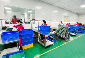
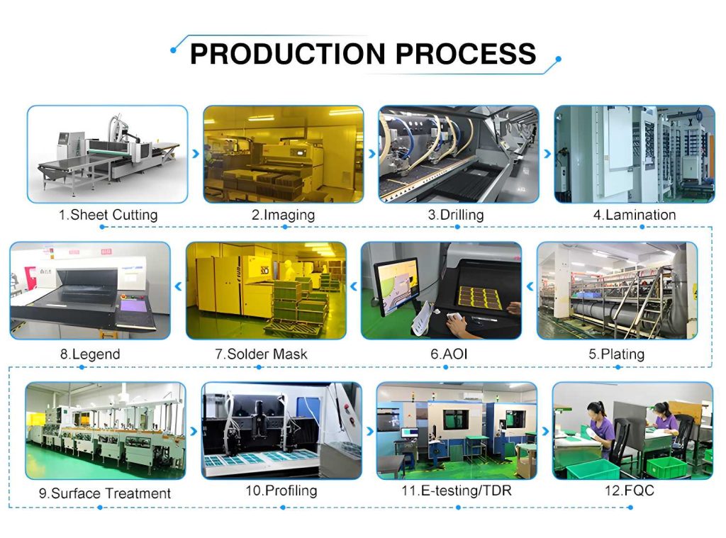
Choosing the right manufacturer for high-frequency PCBs is a critical decision that can significantly impact the success of your project. High-frequency PCBs require a high level of precision and expertise, and selecting a manufacturer with the right skills and experience is essential. When evaluating potential manufacturers, consider factors such as their certifications, quality control processes, and ability to meet your specific requirements. Additionally, consider the importance of prototyping in high-frequency PCB manufacturing, as this step is essential for testing and optimizing the performance of your design before it is committed to production.
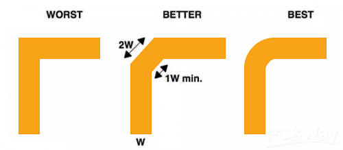
Optimizing trace width and spacing Designers must carefully calculate trace dimensions to maintain consistent impedance and reduce signal degradation.
Using ground planes to reduce electromagnetic interference Extensive ground planes help stabilize reference voltages and diminish interference, creating a cleaner signal path.
Proper via placement to enhance performance Strategic via placement and via types (e.g., blind or buried vias) reduce signal reflections and improve overall circuit efficiency.
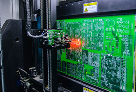
Key evaluations: TDR, impedance verification, and thermal cycling Time Domain Reflectometry (TDR) reveals potential impedance mismatches, while thermal cycling tests confirm a board’s resilience in harsh conditions.
Ensuring signal consistency with advanced testing methods High frequency boards often undergo additional checks such as cross-talk analysis and isolation tests to guarantee peak performance.
Identifying and preventing common failure points By analyzing potential issues—like delamination or poor solder joints—manufacturers can proactively reinforce board reliability.