
In the fast-paced world of electronics, where innovation is the driving force, High-Density Interconnect (HDI) PCBs have emerged as a groundbreaking solution. Whether you’re an engineer designing the next generation of smartphones or a procurement manager sourcing components for a complex project, understanding HDI technology is essential. This guide will take you through everything you need to know about HDI technology, from its basic features to its applications and future trends.
High-Density Interconnect PCBs are a specialized type of printed circuit board (PCB) designed to handle complex electronic systems in compact spaces. Unlike traditional PCBs, HDI technology uses advanced technologies like microvias and stacked layers to maximize space efficiency and improve performance.
In an era where devices are getting smaller and more powerful, HDI technology plays a critical role. It enables manufacturers to pack more functionality into smaller spaces, making it ideal for applications like smartphones, wearables, and medical devices.
If you’re involved in the design, manufacturing, or procurement of electronic devices, this guide is for you. Whether you’re a hardware engineer, a procurement manager, or a company owner, understanding HDI technology will help you make informed decisions.

To truly appreciate the value of HDI technology, it’s important to understand how it differs from traditional PCBs and how it has evolved over time.
Imagine a traditional PCB as a flat surface with electronic components connected by wires. HDI technology, on the other hand, is like a multi-layered cake with tiny tunnels (microvias) connecting each layer. This design allows for more intricate connections in a smaller space.
Traditional PCBs rely on through-hole technology, where components are soldered through drilled holes. HDI technology, however, uses microvias and blind vias, which are smaller and more precise. This results in higher component density and better performance.
PCB technology has come a long way since its inception. Early PCBs were simple and bulky, but as electronic devices became more sophisticated, the need for smaller and more efficient PCBs grew. HDI technology is the result of decades of innovation and refinement.
At the heart of HDI technology are its unique features, which set it apart from other types of PCBs.

Microvias are tiny holes drilled into the PCB to connect different layers. They are much smaller than traditional vias, allowing for more precise routing and higher component density.
HDI technology often has multiple layers stacked in a specific order to maximize space. This stack-up design ensures that components are placed as efficiently as possible, reducing the overall size of the PCB.
The thickness of the copper layers and the width of the traces play a crucial role in the performance of an HDI PCB. Precision engineering ensures that signals travel smoothly and efficiently across the board.
HDI technology is used in a wide range of industries, from consumer electronics to aerospace. Here’s a closer look at some of the most common applications.
Smartphones and wearables are prime examples of devices that rely on HDI technology. Their compact design and high performance make them ideal for these applications.
In the medical field, precision is critical. HDI technology is used in devices like pacemakers and diagnostic equipment, where space and performance are equally important.
The aerospace and defense industries require components that can withstand harsh environments. HDI technology is known for its durability and reliability, making it a popular choice.
Modern vehicles are equipped with advanced electronics, from navigation systems to engine control units. HDI technology plays a crucial role in making these systems compact and efficient.
The benefits of HDI technology are numerous, making it a preferred choice for many applications.
One of the most significant advantages of HDI technology is its ability to save space. By using microvias and stacked layers, it can fit more components into a smaller area.
HDI technology is designed to minimize signal degradation, ensuring that data travels quickly and reliably across the board.
While HDI technology may be more expensive to produce, its ability to reduce overall system size and improve performance often offsets the cost in high-volume applications.
The precise routing and high component density of HDI technology make it ideal for complex circuits, where performance is critical.
Despite their many advantages, HDI technology comes with its own set of challenges.
Designing an HDI PCB requires a high level of precision. Placing microvias in the right locations is essential to ensure proper functionality.
Choosing the right materials is critical. HDI technology needs to be durable enough to withstand harsh environments while remaining flexible enough to accommodate complex designs.
While HDI technology offers many benefits, it is not always the best choice. Cost is a significant factor, and engineers must weigh the advantages against the price.
Even experienced designers can make mistakes. Common issues include improper microvia placement and insufficient testing, both of which can lead to costly errors.
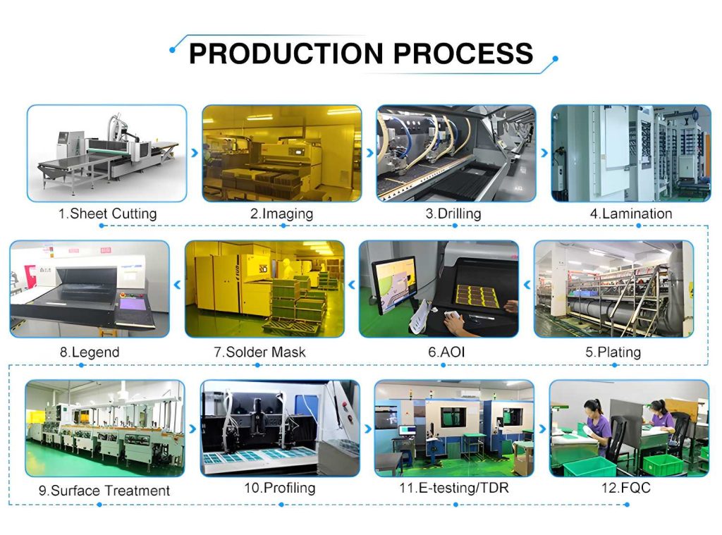
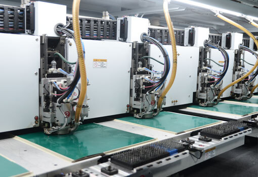
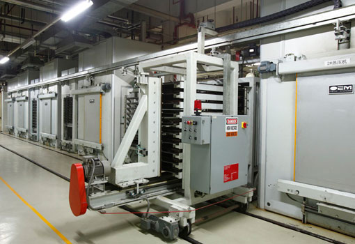
Creating an HDI PCB is a complex process that requires precision at every step.
From designing the layout to drilling microvias and assembling components, each step in the manufacturing process is critical.
Quality control is essential to ensure that each HDI PCB meets the highest standards. This includes testing for signal integrity, durability, and overall performance.
Before an HDI PCB can be used in a device, it must undergo rigorous testing and certification to ensure it meets industry standards.
Selecting the right manufacturer is key to ensuring the success of your HDI PCB project.
When choosing a supplier, consider factors like experience, quality control processes, and production capacity.
Learn from real-world examples of companies that successfully partnered with an HDI PCB manufacturer to achieve their goals.
Before making a decision, ask questions about their capabilities, turnaround time, and quality assurance processes.
The world of HDI technology is constantly evolving, with new technologies and applications on the horizon.
From advanced materials to new manufacturing techniques, the future of HDI technology is bright.
Artificial intelligence and automation are transforming the manufacturing process, making it faster and more efficient.
As technology advances, the demand for HDI technology is expected to grow across various industries.
Here are answers to some common questions about HDI technology.
The advanced technology and precision engineering required to produce HDI PCBs contribute to their higher cost.
Yes, HDI PCBs can be recycled, but the process is more complex than traditional PCBs due to their intricate design.
The production time varies depending on the complexity of the design and the manufacturer’s capabilities.
While HDI technology is ideal for many applications, it may not be the best choice for every industry.
Laser drilling for microvias
Plating and deposition to ensure electrical connectivity
Lamination of multiple layers to create complex structures
Solder mask application for protection and identification
Cutting-edge tools like laser drills enable the precision required for HDI designs. Innovations in plating techniques enhance conductivity and durability.
Ensure reliability through stringent testing like electrical continuity and thermal cycling. Automated optical inspection (AOI) is also used to detect defects early.
| Specifications | PCB Capabilities |
| PCB Layers | 4 ~34 layers |
| High-Density Layers | Up to 18 layers |
| Delivery Time | 1 day to 3 weeks |
| Stackup | 1+N+1, 2+N+2, 3+N+3, 4+N+4 |
| PCB Via | Blind via, Buried via, Staggered via, Stacked via, Skip via |
| Minimum Laser Drill Diameter | 0.075mm |
| Final PCB Thickness | 0.15mm |
| Minimum Trace Width/Space | Flex/rigid-flex PCBs: 1.6mil/1.6mil Rigid PCBs: 3mil/3mil |
| Production Capability | 3000m² per day |
| Copper Thickness | 100μm to 125μm |
| Impedance Control | 90Ω ~100Ω |
| Technical Feature | 90Ω & 100Ω Differential impedance, thick cooper |
| Silkscreen | White, Black, Red,etc. |
| Soldermask | Green, Blue, Purple, White, Black, Pink,Orange |
| Surface finish | OSP, HASL, Lead Free HASL,ENIG,Immersion Tin,Immersion silver, Hard gold plating,etc. |
Choosing onestoppcb for your HDI PCB needs comes with numerous advantages that set us apart in the competitive electronics manufacturing industry:
Speed and Efficiency: Our streamlined manufacturing processes ensure rapid prototyping and on-time delivery, helping you maintain tight project schedules without compromise.
High Precision and Quality: Equipped with state-of-the-art facilities, we specialize in crafting high-density interconnect (HDI) PCBs with unparalleled accuracy and reliability, perfect for sophisticated and compact electronic designs.
Diverse Customization Options: Whether you need multi-layer, blind and buried vias, or microvia solutions, we offer a wide range of configurations to meet your specific requirements.
Global Trust and Expertise: With extensive experience exporting to the U.S., Europe, Vietnam, and South America, we understand and adhere to international standards, ensuring consistent quality every time.
Personalized Support: Our dedicated team of engineers and account managers work closely with you, providing expert guidance and responsive service to simplify your supply chain.
Choosing onestoppcb means partnering with a factory that values speed, diversity, and exceptional quality, ensuring your success in every project.
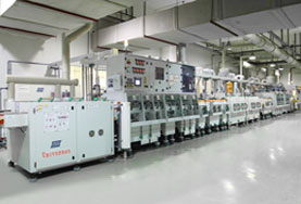

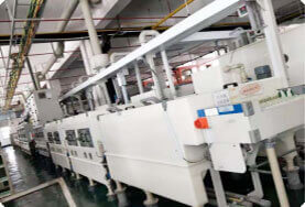
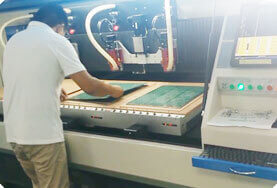
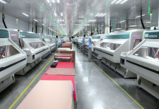
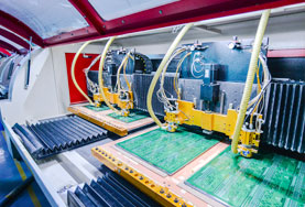
here are more pictures of our factory’s equipment display in our company profile, please click here.
● IATF 16949:2016
● ISO 9001:2015
● ISO14001:2015
● ISO13485:2016
● UL
Furthermore, all our products adhere to the IPC & ROHS Standards. It is our continuous endeavor to produce premium quality PCB products.

We understand you may have questions about our products and services. Here, we provide answers to common queries regarding our HDI PCB.
High-density interconnect, or HDI, circuit boards are printed circuit boards with a higher wiring density per unit area than traditional printed circuit boards.
HDI PCBs differ significantly from standard boards by incorporating multiple layers, micro-vias under 0.008 inches in diameter, and specialized via-in-pad processes. They often include blind, buried, and stacked vias, allowing exceptionally dense circuitry where traces and spaces both measure below 0.005 inches. This combination results in superior miniaturization and performance, making HDI PCBs ideal for mission-critical applications.
Your Trusted HDI PCB Manufacturer Since 2011
onestoppcb brings the advanced capabilities and decades of expertise required to handle all your fabrication and manufacturing needs, including high-density interconnect (HDI) PCBs. With HDI boards gaining increasing popularity across diverse sectors—such as medical, military, and aerospace—we stand ready to deliver the reliability and performance demanded by these critical industries.
PCBs built with high-density interconnect (HDI) technology generally occupy a smaller footprint, as they fit more components into a tighter space. By incorporating blind, buried, and micro vias, along with via-in-pad placements and very fine trace widths, HDI designs efficiently pack a higher component density onto a smaller board.
HDI PCBs deliver substantial advantages. They enable a more compact device footprint and can enhance overall electrical performance, supporting higher data transmission speeds. Moreover, they accommodate more input/output connections within a smaller area.
At onestoppcb, our 4-layer HDI manufacturing process closely resembles standard PCB production, with the primary distinction being the order in which holes are drilled. We start by mechanically drilling buried vias between layers 2 and 3, then move on to the through-holes from layers 1 to 4. Finally, we form blind vias between layers 1-2 and 4-3. This carefully sequenced approach ensures optimal board integrity and reliable signal performance.
At onestoppcb, we use a combination of polymer resin (dielectric)—with or without fillers—reinforcement materials, and metal foil as the primary building blocks of our circuit boards. In a typical layer construction, alternating layers of dielectric and metal foil are stacked to achieve the desired thickness and electrical performance. This process ensures both reliable functionality and structural integrity for a wide range of applications.
We’ve found that PCB dimensions and shape play a crucial role in determining cost. Larger boards require additional materials and take longer to produce, driving up expenses. Meanwhile, PCBs with unusual shapes may need specialized tooling or more complex processes, which can also contribute to higher costs
Simplify your PCB sourcing—get in touch now for high-quality products and efficient service!
ONESTOPPCB
1-4/F Property Office Building, ZhengFeng North Road, Shenzhen, China 518103
Phone: +86-0755-36309132
1-4/F Property Office Building, ZhengFeng North Road, Shenzhen, China 518103
Get in Touch with Onestoppcb – Your Premier PCB Partner
1.Fast Turnaround Time: Our streamlined manufacturing process ensures rapid prototyping and production, meeting tight deadlines effortlessly.
2Diverse Product Range: We offer an extensive variety of PCB types and designs, catering to the unique needs of engineers and procurement teams.
3Quality Assurance: With rigorous quality checks and high standards, we consistently deliver reliable and durable PCBs, minimizing risks for your projects.
Simplify your PCB sourcing—get in touch now for high-quality products and efficient service!