HDI PCB Secrets: Unlocking Next-Level Circuit Density

Introduction: Why Next-Level Circuit Density Matters

The Evolution of PCB Design Over the Decades

The printed circuit board (PCB) has come a long way since its inception. Early PCBs were simple, with through-hole technology dominating the market. However, as electronic devices became more complex and compact, the need for higher circuit density became paramount. This led to the development of High-Density Interconnect (HDI) PCBs, which have revolutionized the way modern electronics are designed and manufactured.

How Miniaturization Drives Innovation in Electronics

Miniaturization is a driving force in the electronics industry. Devices like smartphones, wearables, and medical implants require a high level of functionality packed into a small form factor. HDI PCBs enable this by allowing for more intricate circuit designs within a smaller space, making them indispensable in today’s tech-driven world.

Core Concepts of High-Density Interconnect

Understanding Microvias, Blind Vias, and Buried Vias

HDI PCB Mirovia

HDI PCBs rely on advanced via technologies to achieve higher circuit density. Microvias are tiny holes that connect different layers of the PCB, significantly reducing the overall size of the board. Blind vias connect the surface layer to an internal layer, while buried vias link internal layers without reaching the surface. These technologies enable more precise routing and higher component density.

Layer Stacking and Sequential Lamination Basics

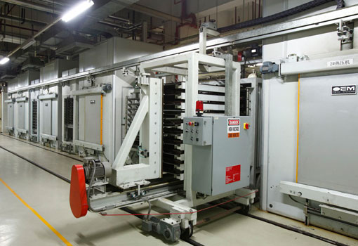
HDI PCBs often use sequential lamination, where layers are added one at a time. This process allows for precise control over layer thickness and alignment, ensuring optimal performance. Layer stacking involves arranging layers in a specific order to maximize space efficiency and improve signal integrity.

Critical Material Considerations

Dielectrics and Their Role in Signal Integrity

The choice of dielectric material is crucial for maintaining signal integrity in HDI PCBs. High-performance dielectrics with low loss tangents are essential for reducing signal degradation and ensuring reliable data transmission. Additionally, dielectrics must have sufficient thermal stability to withstand the manufacturing process and operational conditions.

Matching Copper Weights and Surface Treatments

Copper weight and surface treatment play a significant role in the performance of HDI PCBs. The thickness of copper layers affects trace width and current-carrying capacity. Surface treatments like immersion gold or organic solderability preservatives (OSP) protect the board from oxidation and ensure reliable solder joints.

Advanced Manufacturing Techniques

Laser Drilling and Precision Etching

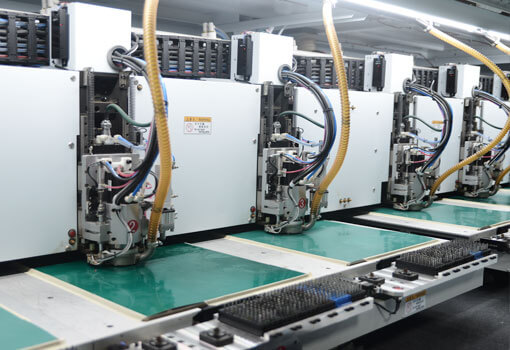
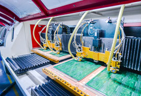
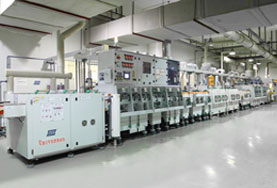
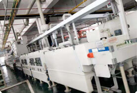
Laser drilling is a key technique in HDI PCB manufacturing. It allows for the creation of microvias with high precision and minimal thermal damage. Precision etching is another critical process, ensuring that traces are uniform and meet design specifications. These techniques require advanced equipment and skilled operators to achieve the desired results.

Plating Processes for Enhanced Reliability

Plating processes, such as electroless nickel immersion gold (ENIG), are used to enhance the reliability of HDI PCBs. These processes provide a robust surface finish that resists corrosion and ensures long-term performance. Proper plating techniques are essential for maintaining signal integrity and mechanical durability.

Overcoming Design Challenges

Managing Signal Noise and Crosstalk in Tight Spaces

One of the challenges in HDI PCB design is managing signal noise and crosstalk, especially in densely packed circuits. Proper routing techniques, such as differential pairs and ground planes, can help mitigate these issues. Additionally, careful placement of components and vias can reduce electromagnetic interference (EMI).

Balancing Trace Width, Spacing, and Via Density

Achieving the right balance between trace width, spacing, and via density is crucial for optimal performance. Narrower traces and tighter spacing allow for higher circuit density, but they also increase the risk of signal degradation. Designers must use advanced simulation tools to ensure that the circuit meets performance requirements while maintaining manufacturability.

Cost-Effective Approaches to Compact Boards

Strategies for Minimizing Production Costs

While HDI PCBs offer many benefits, they can be more expensive to produce than traditional PCBs. Strategies for minimizing costs include optimizing the design for manufacturability, choosing cost-effective materials, and leveraging economies of scale in high-volume production. Additionally, manufacturers can reduce costs by minimizing waste and streamlining the production process.

Deciding Between Single- vs. Multiple-Lamination Cycles

The number of lamination cycles can significantly impact the cost and complexity of HDI PCB production. Single-cycle lamination is simpler and less expensive, but it may not be suitable for all designs. Multiple-cycle lamination allows for more complex layer arrangements but increases production time and cost. Choosing the right approach depends on the specific requirements of the project.

Applications That Demand Higher Density

Shrinking Consumer Electronics and Wearables

Consumer electronics, such as smartphones and wearables, are prime examples of applications that demand higher circuit density. These devices require compact designs with high functionality, making HDI PCBs an ideal choice. The ability to pack more components into a smaller space enables manufacturers to create devices that are both powerful and portable.

Automotive, Medical, and Aerospace Requirements

In industries like automotive, medical, and aerospace, reliability and performance are critical. HDI PCBs are used in advanced driver-assistance systems (ADAS), medical implants, and avionics, where space constraints and high-performance requirements are common. The durability and precision of HDI PCBs make them well-suited for these demanding applications.

Testing and Quality Control Essentials

Automated Optical Inspection and X-Ray Analysis

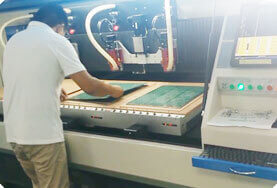
Testing and quality control are essential for ensuring the reliability of HDI PCBs. Automated optical inspection (AOI) and X-ray analysis are commonly used to detect defects and verify that the board meets design specifications. These techniques provide high accuracy and are capable of inspecting complex structures that are difficult to assess visually.

Ensuring Mechanical and Thermal Durability

HDI PCBs must withstand mechanical stresses and thermal variations over their operational lifespan. Testing for mechanical durability includes bending and vibration tests, while thermal tests evaluate the board’s performance under different temperature conditions. Ensuring that HDI PCBs meet these requirements is critical for their success in real-world applications.

Future Trends in Circuit Miniaturization

Next-Generation Materials on the Horizon

As technology advances, new materials are being developed that could further enhance HDI PCB performance. Materials with higher thermal conductivity, lower dielectric loss, and improved mechanical properties are on the horizon. These materials could enable even more compact and efficient circuit designs.

Potential of Embedded Components and 3D Structures

The integration of embedded components and 3D structures is another exciting trend in HDI PCB technology. Embedded components reduce the need for surface-mounted parts, further shrinking the overall size of the board. 3D structures, such as stacked dies and multi-layer configurations, offer new possibilities for high-density interconnects.

Prototyping and Bringing It All Together

Best Practices for First-Run Boards

Prototyping is a critical step in the development of HDI PCBs. Best practices include using high-quality materials, collaborating with experienced manufacturers, and conducting thorough testing. First-run boards should be evaluated for performance, reliability, and manufacturability to ensure that the final product meets design specifications.

Partnering with Specialized Fabricators for Success

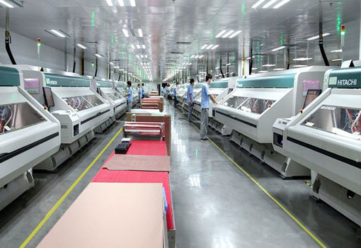
Working with specialized fabricators is essential for the successful production of HDI PCBs. These fabricators have the expertise, equipment, and processes needed to handle the complexity of HDI technology. Partnering with a trusted fabricator can help ensure that the project is completed on time, within budget, and to the highest standards of quality.

Conclusion

HDI PCBs have become a cornerstone of modern electronics, enabling the miniaturization and performance improvements that drive innovation. From consumer devices to high-reliability applications in automotive, medical, and aerospace, HDI technology offers unparalleled benefits. As the industry continues to evolve, new materials, manufacturing techniques, and design approaches will further enhance the capabilities of HDI PCBs, shaping the future of electronics.

Call to Action: Partner with Experts for Your Next HDI PCB Project

Ready to explore the possibilities of HDI technology? Start by consulting with a trusted fabricator who specializes in HDI PCB production. Their expertise can help you unlock the full potential of high-density interconnects and bring your next-generation designs to life.

Table of Contents

Contact Us

Simplify your PCB sourcing—get in touch now for high-quality products and efficient service!

Our HDI PCB Fabrication Capacity

SpecificationsPCB Capabilities
PCB Layers4 ~34 layers
High-Density LayersUp to 18 layers
Delivery Time1 day to 3 weeks
Stackup1+N+1, 2+N+2, 3+N+3, 4+N+4
PCB ViaBlind via, Buried via, Staggered via, Stacked via, Skip via
Minimum Laser Drill Diameter0.075mm
Final PCB Thickness0.15mm
Minimum Trace Width/SpaceFlex/rigid-flex PCBs: 1.6mil/1.6mil
Rigid PCBs: 3mil/3mil
Production Capability3000m² per day
Copper Thickness100μm to 125μm
Impedance Control90Ω ~100Ω
Technical Feature90Ω & 100Ω Differential impedance, thick cooper
SilkscreenWhite, Black, Red,etc.
SoldermaskGreen, Blue, Purple, White, Black, Pink,Orange
Surface finishOSP, HASL, Lead Free HASL,ENIG,Immersion Tin,Immersion silver, Hard gold plating,etc.

Our HDI PCB Lamination and Drilling Equipment

Drilling production line at RF PCB Manufacturer
Drilling production line
High-speed six-axis drilling machine at RF PCB Manufacturer
High-speed six-axis drilling machine
Press machine
Press machine
CNC machine
CNC Plate Forming

Why Choose Onestoppcb's HDI PCB Manufacturing Services

Choosing onestoppcb for your HDI PCB needs comes with numerous advantages that set us apart in the competitive electronics manufacturing industry:

  1. Speed and Efficiency: Our streamlined manufacturing processes ensure rapid prototyping and on-time delivery, helping you maintain tight project schedules without compromise.

  2. High Precision and Quality: Equipped with state-of-the-art facilities, we specialize in crafting high-density interconnect (HDI) PCBs with unparalleled accuracy and reliability, perfect for sophisticated and compact electronic designs.

  3. Diverse Customization Options: Whether you need multi-layer, blind and buried vias, or microvia solutions, we offer a wide range of configurations to meet your specific requirements.

  4. Global Trust and Expertise: With extensive experience exporting to the U.S., Europe, Vietnam, and South America, we understand and adhere to international standards, ensuring consistent quality every time.

  5. Personalized Support: Our dedicated team of engineers and account managers work closely with you, providing expert guidance and responsive service to simplify your supply chain.

Choosing onestoppcb means partnering with a factory that values speed, diversity, and exceptional quality, ensuring your success in every project.

Equipment at onestoppcb

here are more pictures of our factory’s equipment display in our company profile, please click here.

Our Certifications

We are duly certified with the following accreditations:

● IATF 16949:2016
● ISO 9001:2015
● ISO14001:2015
● ISO13485:2016
● UL

Furthermore, all our products adhere to the IPC & ROHS Standards. It is our continuous endeavor to produce premium quality PCB products.

certifications

FAQ

Common Questions and Answers

We understand you may have questions about our products and services. Here, we provide answers to common queries regarding our HDI PCB.

What is HDI in PCB?

High-density interconnect, or HDI, circuit boards are printed circuit boards with a higher wiring density per unit area than traditional printed circuit boards.

HDI PCBs differ significantly from standard boards by incorporating multiple layers, micro-vias under 0.008 inches in diameter, and specialized via-in-pad processes. They often include blind, buried, and stacked vias, allowing exceptionally dense circuitry where traces and spaces both measure below 0.005 inches. This combination results in superior miniaturization and performance, making HDI PCBs ideal for mission-critical applications.

Your Trusted HDI PCB Manufacturer Since 2011

onestoppcb brings the advanced capabilities and decades of expertise required to handle all your fabrication and manufacturing needs, including high-density interconnect (HDI) PCBs. With HDI boards gaining increasing popularity across diverse sectors—such as medical, military, and aerospace—we stand ready to deliver the reliability and performance demanded by these critical industries.

PCBs built with high-density interconnect (HDI) technology generally occupy a smaller footprint, as they fit more components into a tighter space. By incorporating blind, buried, and micro vias, along with via-in-pad placements and very fine trace widths, HDI designs efficiently pack a higher component density onto a smaller board.

HDI PCBs deliver substantial advantages. They enable a more compact device footprint and can enhance overall electrical performance, supporting higher data transmission speeds. Moreover, they accommodate more input/output connections within a smaller area.

What is the HDI PCB manufacturing process?

At onestoppcb, our 4-layer HDI manufacturing process closely resembles standard PCB production, with the primary distinction being the order in which holes are drilled. We start by mechanically drilling buried vias between layers 2 and 3, then move on to the through-holes from layers 1 to 4. Finally, we form blind vias between layers 1-2 and 4-3. This carefully sequenced approach ensures optimal board integrity and reliable signal performance.

At onestoppcb, we use a combination of polymer resin (dielectric)—with or without fillers—reinforcement materials, and metal foil as the primary building blocks of our circuit boards. In a typical layer construction, alternating layers of dielectric and metal foil are stacked to achieve the desired thickness and electrical performance. This process ensures both reliable functionality and structural integrity for a wide range of applications.

We’ve found that PCB dimensions and shape play a crucial role in determining cost. Larger boards require additional materials and take longer to produce, driving up expenses. Meanwhile, PCBs with unusual shapes may need specialized tooling or more complex processes, which can also contribute to higher costs

Contact Us

Simplify your PCB sourcing—get in touch now for high-quality products and efficient service!

Get In Touch With Us

Get in Touch with Onestoppcb – Your Premier PCB Partner

1.Fast Turnaround Time: Our streamlined manufacturing process ensures rapid prototyping and production, meeting tight deadlines effortlessly.

2Diverse Product Range: We offer an extensive variety of PCB types and designs, catering to the unique needs of engineers and procurement teams.

3Quality Assurance: With rigorous quality checks and high standards, we consistently deliver reliable and durable PCBs, minimizing risks for your projects.

Contact Us

Simplify your PCB sourcing—get in touch now for high-quality products and efficient service!