High Frequency Pcb

High-Frequency Pcb (OneStoppcb)

1. Introduction to Advanced Circuit Boards

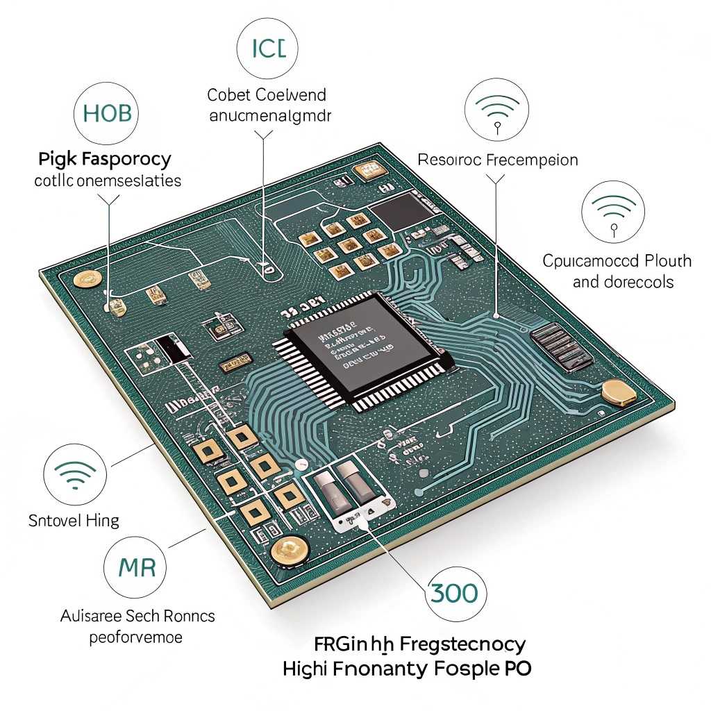
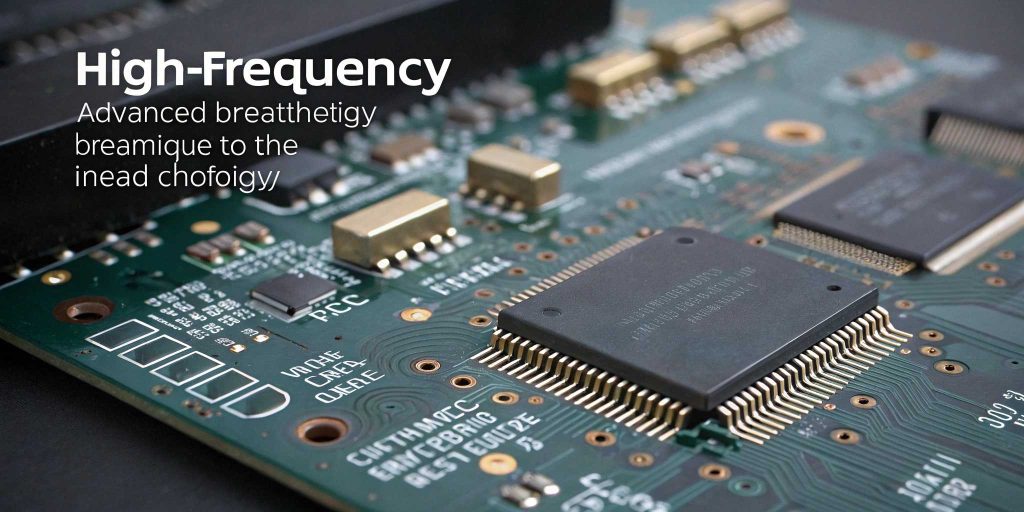
What makes these boards different from standard ones? High frequency PCBs are engineered to handle high-speed signals and microwaves beyond the range of standard boards. They rely on specialized materials with low dielectric constants and minimal signal loss, ensuring reliability in demanding applications.

Their role in modern electronics In an era where devices require faster processing and seamless connectivity, high frequency PCBs serve as the backbone of advanced systems, powering everything from high-speed communication tools to innovative consumer electronics.

Key industries benefiting from advanced circuit technology Industries such as telecommunications, aerospace, and automotive rely heavily on high frequency PCBs to deliver precision, efficiency, and consistent performance in mission-critical operations.high frequency pcb Characteristics

2. Essential Applications in Various Sectors

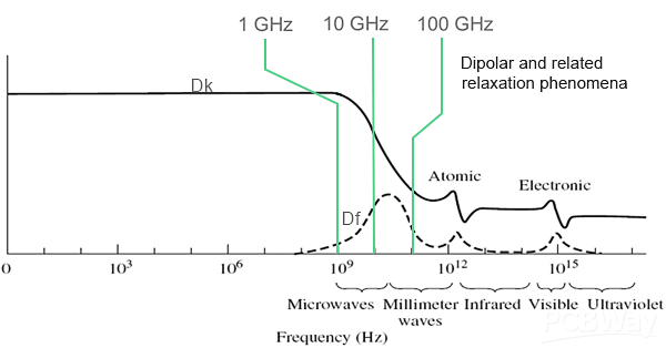
Telecommunications and RF systems High frequency PCBs enable rapid data transmission with minimal interference, making them a cornerstone in telecom infrastructure, wireless devices, and communication satellites.

Aerospace and military innovations In environments where reliability is non-negotiable, high frequency PCBs ensure stable signals. They withstand extreme conditions and are integral to avionics, radar systems, and defense electronics.

Medical devices and automotive electronics Precise data handling and robust performance are crucial in medical diagnostic equipment and automotive safety systems. High frequency PCBs help deliver accurate, real-time monitoring and control.

The growing impact on IoT and wireless solutions As the Internet of Things evolves, more smart devices require high speed data processing and wireless connectivity. High frequency PCBs play a pivotal role in enabling this interconnected ecosystem.

3. Key Materials and Their Importance

Comparing PTFE (Teflon) and FR4 materials PTFE materials, known for their low dielectric constant, are common in high frequency boards, ensuring minimal signal loss. In contrast, FR4 is cost-effective and widely used but may not provide the same precision.

How dielectric constant (Dk) affects performance A material’s Dk determines how well it supports high-speed signals. A lower Dk typically translates to reduced signal attenuation, greater efficiency, and better overall performance.

Selecting the right material for signal integrity Choosing the ideal substrate often involves balancing cost, operational frequency requirements, and the specific demands of the application.


4. Crucial Design Considerations

Maintaining impedance control for reliability Precise impedance control is critical to prevent signal distortions. Designers must consider trace width, spacing, and layer arrangement to ensure optimal signal integrity.

Reducing interference and crosstalk issues Proper grounding and shielding techniques help to minimize electromagnetic interference, improving signal clarity and device longevity.

Effective layer stack-up strategies for optimal function Layer stack-ups can significantly influence performance. A well-planned configuration reduces interference, simplifies routing, and improves mechanical stability.

5. Overcoming Manufacturing Challenges

Achieving precise etching for signal traces High frequency signals demand accurate trace width control. Manufacturers use advanced etching processes and meticulous quality checks to meet tight tolerances.

Managing thermal expansion in various environments Disparate materials may expand differently under heat. Selecting compatible materials and carefully engineering the board can prevent cracks and signal losses.

Selecting the right production partner for complex boards Partnering with a specialized manufacturer experienced in high frequency PCB production is paramount to success, ensuring efficient processes and high yields.

OneStoppcb High Frequency PCB Fabrication Capacity

 Feature Capability
 Layer Counts 1-36
 Normal Lead Time 4-6 Working Days
 Fast Lead Time 1-2 Working Days
 Materials ISOLA, Shengyi, Rogers,
Nelco, Arlon etc.
 Copper Thickness(Finished) 1/3OZ-20OZ
 Overall Board Thickness 0.2-5MM
 Minimum Line/Track Width & Space 3Mil/3Mil
 Solder Mask Color Green,black,blue.white,
red,yellow. glossy and matt etc.
 Legend/Silkscreen Color White, yellow, black, etc
 Back drilling ≤16mil
 Surface Treatment Plating Gold, ENIG, Immersion
Tin&Silver etc.
 Qualifications UL, ISO 14001:2015  IS9001:2015Certified

Manufacturing Process

Pcb Production Process

Need an Instant Quote For Your Upcoming Project?

Send us the details and we will get back to you within 12 hours

6. Best Practices for Routing and Layout

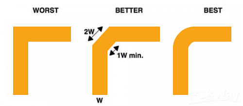
Optimizing trace width and spacing Designers must carefully calculate trace dimensions to maintain consistent impedance and reduce signal degradation.

Using ground planes to reduce electromagnetic interference Extensive ground planes help stabilize reference voltages and diminish interference, creating a cleaner signal path.

Proper via placement to enhance performance Strategic via placement and via types (e.g., blind or buried vias) reduce signal reflections and improve overall circuit efficiency.


7. Testing and Quality Assurance Strategies

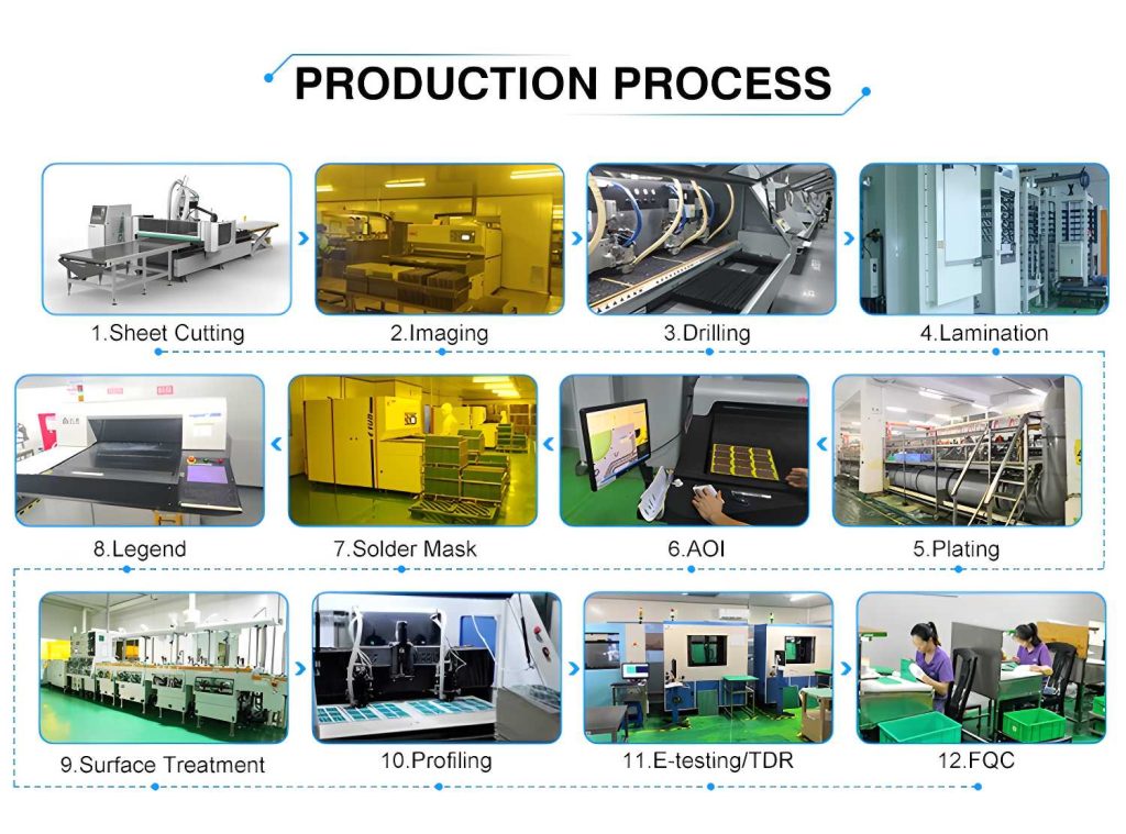
Key evaluations: TDR, impedance verification, and thermal cycling Time Domain Reflectometry (TDR) reveals potential impedance mismatches, while thermal cycling tests confirm a board’s resilience in harsh conditions.

Ensuring signal consistency with advanced testing methods High frequency boards often undergo additional checks such as cross-talk analysis and isolation tests to guarantee peak performance.

Identifying and preventing common failure points By analyzing potential issues—like delamination or poor solder joints—manufacturers can proactively reinforce board reliability.

Our Test Machine and Process

Flying probe test machine-high Frequency pcb
Flying probe test machine
Automatic testing machine
Test machine-High Frequency Pcb

Test Detail

FQC finished product inspection
There are more pictures of our factory’s equipment display in our company profile, please click here.

8. Cost Factors and Budgeting Smartly

How material selection influences pricing Advanced substrates like PTFE tend to be more expensive but deliver superior performance for specialized applications.

Balancing performance needs with affordability Understanding the trade-offs between lower-cost materials and high-end substrates is essential. A thorough ROI analysis helps in selecting the ideal option.

When to invest in next-generation solutions For designs pushing limits in speed, bandwidth, or operating environment, next-gen materials and processes can provide significant advantages in the long run.


9. Future Innovations in Circuit Board Technology

The role of 5G and emerging wireless trends As 5G networks expand, the demand for high frequency PCBs will surge, spurring further research into advanced materials and designs.

Advances in material science for next-gen designs New polymers, ceramics, and hybrid compositions aim to offer superior performance while maintaining cost-effectiveness.

AI and automation shaping manufacturing processes Automated inspection, machine learning-driven process controls, and robotic assembly lines will continue to elevate precision and throughput.


Our Certification

We are duly certified with the following accreditations:

● IATF 16949:2016
● ISO 9001:2015
● ISO14001:2015
● ISO13485:2016
● UL

Furthermore, all our products adhere to the IPC & ROHS Standards. It is our continuous endeavor to produce premium quality PCB products

certifications

FAQ

Common Questions and Answers

We understand you may have questions about our products and services. Here, we provide answers to common queries regarding our HIGH FREQUENCY PCB.

What are high-frequency PCBs?

High Frequency Printed Circuit Boards (HF PCBs) rely on specially engineered substrates to reliably handle signals beyond 500MHz with minimal attenuation. Thanks to this robust performance, they’re a critical component in telecom and RF microwave systems, as well as in demanding military and aerospace applications that require precision and signal integrity.

High-frequency PCBs mainly address transmission efficiency and reduced signal loss, whereas high-speed PCBs emphasize maintaining signal integrity, accurate timing, and noise mitigation. Thus, choosing the right PCB type for your specific application is vital for robust performance and reliability.

Products that may contain PCBs include:
  • Transformers and capacitors.
  • Electrical equipment including voltage regulators, switches, re-closers, bushings, and electromagnets.
  • Oil used in motors and hydraulic systems.
  • Old electrical devices or appliances containing PCB capacitors.
  • Fluorescent light ballasts.
  • Cable insulation.

A standard guideline recommends that the ground plane extend roughly twenty times the board’s thickness (H) beyond the region of the signal traces or power planes. Essentially, this means setting the traces and power planes back by about 20H from the ground plane edges.

Is high-frequency current safe?

High-frequency electricity remains dangerous and can potentially cause severe burns. Fundamentally, it’s the voltage that drives current and causes harm, a principle that holds true regardless of frequency.

In high-frequency treatments, additional oxygen molecules are generated, yielding an antibacterial effect and a gentle warming of the tissues. This process supports blood vessels in eliminating toxins, while skin cells gain extra nutrients and increased hydration.

Signals typically operating between 50 MHz and 3 GHz are prone to issues with signal integrity, power integrity, and EMI. Therefore, when frequencies exceed 50 MHz, strict adherence to high-speed PCB design rules is crucial. Boards handling these higher frequencies are generally classified as high-speed PCBs.

Maintaining impedance control for reliability Precise impedance control is critical to prevent signal distortions. Designers must consider trace width, spacing, and layer arrangement to ensure optimal signal integrity.

Reducing interference and crosstalk issues Proper grounding and shielding techniques help to minimize electromagnetic interference, improving signal clarity and device longevity.

Effective layer stack-up strategies for optimal function Layer stack-ups can significantly influence performance. A well-planned configuration reduces interference, simplifies routing, and improves mechanical stability.

Minimizing high-frequency interference requires strategic layout, optimized layer stack-up, and precise grounding. Use continuous ground planes, keep critical traces short, and ensure each signal references a low-impedance return path. Decoupling capacitors near power pins help filter noise, while thoughtful spacing of analog and digital circuits avoids crosstalk. Proper impedance control and shielding techniques also play key roles.

Request A Free Quote

We'd like to work with you

Send us a message if you have any questions or request a quote. Our experts will give you a reply within 24 hours and help you select the right valve you want.